The view that AI is inseparable from HBM (High Bandwidth Memory) is increasingly taking root in people's minds.
For the training of large AI models, a large amount of parallel data processing requires high computing power and high bandwidth. Computing power determines the speed of data processing per second, while bandwidth determines the amount of data that can be accessed per second. GPUs are responsible for providing computing power, and memory is responsible for providing bandwidth.
The current situation is that while everyone can do without NVIDIA's GPUs, they absolutely cannot do without HBM from Hynix, Samsung, or Micron. Although NVIDIA has the moat of CUDA, it cannot completely prevent users from migrating to other manufacturers. However, HBM is different. Whether it is AMD, Intel, or other custom chips, they all have dense HBM embedded in them without exception.
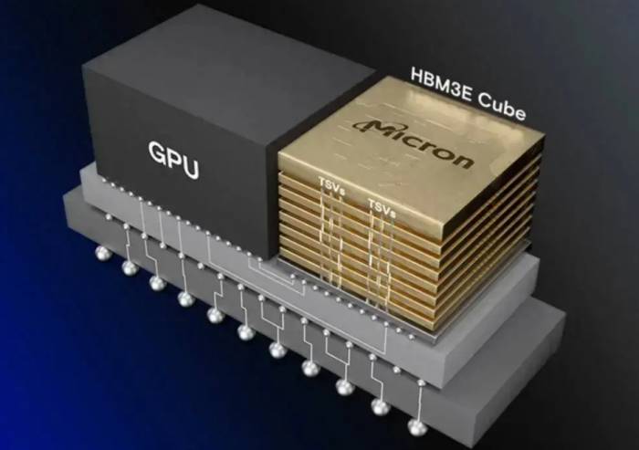
But HBM is not ordinary DRAM, and its price has already reached a staggering level. Under the same density, the price of HBM is about 5 times that of DDR5. It is understood that the current cost of HBM ranks third in the cost of AI servers, accounting for about 9%, with an average unit price as high as 18,000 US dollars.
(The picture is from Micron)
Even such expensive HBM is still in a state of supply shortage and is still rising in price. TrendForce said in May this year that the 2025 HBM pricing negotiations have started in the second quarter of 2024. However, due to the limited overall capacity of DRAM, suppliers have initially increased prices by 5% to 10% to manage capacity constraints, affecting HBM2e, HBM3, and HBM3e.
Advertisement
It pointed out that from the perspective of major AI solution providers, the demand for HBM specifications will clearly shift towards HBM3e, and the expected increase in 12Hi stacked products will drive the increase in single-chip HBM capacity. It is estimated that the annual growth rate of HBM demand in 2024 will approach 200%, and it is expected to double again in 2025.
Giants who can afford the money will continue to bid up for larger-capacity HBM, but for small and medium-sized manufacturers, the expensive HBM has become the biggest obstacle on their way to large models.
Who will come to the rescue for the expensive AI memory?Silicon Sage Aims to Bring Down Memory Prices
The "Silicon Sage," Jim Keller, has criticized the high prices of current AI chips on more than one occasion.
Who is Jim Keller? His career spans DEC, AMD, SiByte, Broadcom, PA Semi, Apple, Tesla, and Intel. From AMD's K8 architecture, to Apple's A4 and A5 processors, to AMD's Zen architecture, and finally to Tesla's FSD autonomous driving chip, this mastermind has been behind the scenes.
In 2021, he left Intel and joined the AI chip startup Tenstorrent in Toronto, Canada, as the company's CTO, responsible for developing the next generation of AI chips.
Keller has been committed to addressing the high cost of artificial intelligence hardware, seeing it as an entry point for startups like Tenstorrent to challenge giants like Nvidia. He once proposed that Nvidia could have saved $1 billion in the development of the Blackwell GPU if they had used Ethernet interconnect technology.
"There are many markets that are not well served by Nvidia," Keller said in an interview with Nikkei Asia. As the application of AI in smartphones, electric vehicles, and cloud services continues to expand, more and more companies are looking for cheaper solutions. He mentioned, "There are many small companies that are unwilling to pay $20,000 to purchase Nvidia's high-end GPUs, which are considered the best choice in the market."
Tenstorrent is preparing to sell its second-generation multifunctional AI chip by the end of this year. The company claims that in some areas, its energy efficiency and processing efficiency are superior to Nvidia's AI GPUs. According to Tenstorrent, the efficiency of its Galaxy system is three times that of Nvidia's AI server DGX, and the cost has been reduced by 33%.
One of the reasons for this achievement, Keller said, is that the company does not use high-bandwidth memory (HBM), an advanced memory chip that can quickly transfer large amounts of data. HBM is an important component of generative AI chips and has played a significant role in the success of Nvidia's products.
However, HBM is also one of the main culprits of high energy consumption and high prices of AI chips. "Even those who use HBM are struggling with its cost and design time," Keller said. Therefore, he made the technical decision not to use this technology.
In a typical AI chip set, the GPU sends data to memory during each execution process. This requires the high-speed data transfer capability of HBM. However, Tenstorrent has specifically designed its chips to significantly reduce such transfers. Keller said that through this new approach, the company's designed chips can replace GPUs and HBM in some areas of AI development.He also stated that the company is designing its products to achieve "cost-effectiveness" as much as possible. He added that many other companies are also looking for better memory solutions, but he cautiously acknowledged that it would take several years to disrupt the existing large High Bandwidth Memory (HBM) industry.
Keller predicted that more new players would emerge to fill the various AI markets that Nvidia failed to serve, rather than being replaced by a single company.
It is worth mentioning that Tenstorrent's Chief CPU Architect has also shared similar views, emphasizing that the company's more pragmatic and economical spirit makes its system design more cost-effective and computationally powerful than Nvidia.
He said, "Customers do not need to pay the price of a Porsche or Ferrari to run their generative AI models; they just need the most cost-effective and fastest-running car." Lien expects that the current trend of expensive hardware prices will gradually fade away, and the market will eventually stabilize.
For Jim Keller, the overly expensive HBM seems to have hindered the development of AI. Although large companies have the financial strength to bear the costs, small companies have long been unable to sustain it. The Tenstorrent chip he is responsible for is designed to solve this problem.
AI chips without HBM?
In May 2020, Tenstorrent launched its first product - Grayskull, a processor based on the GF 12nm process, approximately 620 square millimeters, initially designed as an inference accelerator and host. It contains 120 custom cores with a 2D bidirectional mesh structure, providing 368 TeraOPs of 8-bit computing power with a power consumption of only 65 watts. Each custom core is equipped with a data-controlled packet management engine, a packet computing engine containing Tenstorrent's custom TENSIX cores, and five RISC cores for non-standard operations (such as conditional statements). The chip focuses on sparse tensor operations, optimizing matrix operations into compressed data packets, and achieving pipeline parallelism of computational steps through a graphics compiler and packet manager. This also enables dynamic graph execution, allowing for asynchronous computation and data transfer compared to some other AI chip models, rather than specific computation/transfer time domains.
In March of this year, Tenstorrent began selling two development boards based on Grayskull. Tenstorrent stated that Grayskull e75 and e150 are Tenstorrent's foundational, inference-only AI graphics processors, each built with Tensix Cores, including a computational unit, on-chip network, local cache, and "small RISC-V" core, achieving unique and efficient data movement within the chip, designed for adventurous ML developers seeking cost-effective, customizable traditional GPU alternatives.
The Grayskull e75 is a 75-watt PCIe Gen 4 card priced at $600, featuring a 1GHz NPU chip with 96 Tensix cores and 96MB of SRAM. The board also includes 8GB of standard LPDDR4 DRAM. The Grayskull e150 increases the clock frequency to 1.2GHz, the number of cores to 120, and the on-chip memory to 120MB accordingly, but the off-chip DRAM remains at 8GB of LPDDR4, with a power consumption increase to 200 watts and a price of $800.
It is understood that the Tenstorrent Grayskull architecture is different from other data center AI accelerators (GPU/NPU). The arranged Tensix cores contain multiple CPUs for the computational unit, which includes vector and matrix engines. This structured granular approach can increase the utilization rate of mathematical units, thereby improving performance per watt. Each Tensix core also has 1MB of SRAM, providing an ample total on-chip memory. Unlike other NPUs with large memory, Grayskull can be connected to external memory.Of course, the most important aspect is that Grayskull uses standard DRAM instead of expensive HBM, which alone saves a significant portion of the cost, aligning with Jim Keller's mentioned goal of pursuing cost-effectiveness.
Software is a weak link for NPU and other processor challengers, but it is a strength for Grayskull compared to its competitors. Tenstorrent offers two software workflows for this: TT-Buda maps models to Tenstorrent hardware based on standard AI frameworks such as PyTorch and TensorFlow, while TT-Metalium provides developers with direct hardware access and allows them to create libraries for more advanced frameworks. With the support of the Grayskull architecture, Metalium stands out for offering a computer-like programming model and may attract customers with low-level programming resources.
In addition, from the start, Tenstorrent has taken power efficiency as a differentiating factor, with the relatively low 75 watts of e75, conforming to the standard PCIe and OCP power range. A design like this could be a great server add-on board for the inference field. In addition to the Grayskull chip and board, Tenstorrent has also begun to license its high-performance RISC-V CPU and Tensix cores, and co-develop Chiplets with partners.
Of course, this is just the beginning. After Jim Keller joined, Tenstorrent's ambitions began to grow larger.
In July of this year, Tenstorrent launched a new generation of Wormhole processors, designed specifically for AI workloads, promising good performance at a low price. The company currently offers two additional PCIe cards, each equipped with one or two Wormhole processors, as well as TT-LoudBox and TT-QuietBox workstations, designed specifically for software developers. This release is mainly aimed at developers, not those who use Wormhole boards for commercial workloads.
Tenstorrent CEO Jim Keller said, "It is always satisfying to get more products into the hands of developers. The release of the Wormhole card development system helps developers expand and develop multi-chip AI software. In addition to this release, we are also very pleased with the smooth tape-out and launch progress of the second-generation product Blackhole."
Each Wormhole processor is equipped with 72 Tensix cores (including five RISC-V cores supporting various data formats), has 108MB of SRAM, and provides a performance of 262 FP8 TFLOPS at a frequency of 1GHz, with a power consumption of 160W. The single-chip Wormhole n150 card is equipped with 12GB of GDDR6 memory, with a bandwidth of 288GB/s.
Wormhole processors offer flexible scalability to meet the needs of various workloads. In a standard workstation setup, four Wormhole n300 cards can be merged into one unit, displayed as a unified, extensive Tensix core network in the software. This configuration allows the accelerator to process the same workload, assigned to four developers, or run up to eight different AI models simultaneously. A key feature of this scalability is that it can run natively without virtualization. In a data center environment, Wormhole processors can be expanded within a machine through PCIe or between multiple machines through Ethernet.
From a performance perspective, Tenstorrent's single-chip Wormhole n150 card (72 Tensix cores, 1GHz, 108MB SRAM, 12GB GDDR6, bandwidth of 288GB/s) provides 262 FP8 TFLOPS at a power consumption of 160W, while the dual-chip Wormhole n300 board (128 Tensix cores, 1GHz, 192MB SRAM, 24GB GDDR6, bandwidth of 576GB/s) can provide up to 466 FP8 TFLOPS at a power consumption of 300W (according to Tom's Hardware data).
Compared with Nvidia's products, Nvidia's A100 does not support FP8 but supports INT8, with a peak performance of 624 TOPS (1,248 TOPS when sparse), while Nvidia's H100 supports FP8, with a peak performance of up to 1,670 TFLOPS (3,341 TFLOPS when sparse), which is a significant gap compared to Tenstorrent's Wormhole n300.However, the price compensates for the lack of performance. Tenstorrent's Wormhole n150 is priced at $999, while the n300 is priced at $1,399. In comparison, the price of a single Nvidia H100 card could reach up to $30,000.
In addition to the cards, Tenstorrent also offers developers workstations pre-installed with four n300 cards, including the lower-priced Xeon-based TT-LoudBox and the high-end EPYC-based TT-QuietBox.
Whether it is Grayskull or Wormhole, they are just the first step in Tenstorrent's roadmap, and the real highlight is still to come.
(The image is from Tenstorrent)
According to the roadmap disclosed by Tenstorrent, the second-generation Blackhole chip has 140 Tensix cores, as well as more DRAM and faster Ethernet, and has 16 RISC-V cores, which are independent of the Tensix cores and can run the operating system without an x86 CPU. It has been taped out on TSMC N6 and is progressing smoothly.
Tenstorrent's third-generation architecture will be based on chipsets and will migrate to Samsung SF4, which includes Quasar and Grendel, and will use updated Tensix cores. The goal is to gather four Tensix cores with shared L2 to better reuse the weights already in memory. They are expected to be launched in 2025.
Of course, the three chips in the later part of the roadmap all do not use HBM, but choose GDDR6 instead. Both Tenstorrent and Jim Keller have a goal, that is, to break the expensive myth of HBM.
A niche solution to take a detour
Tenstorrent is not the only company that wants to replace HBM with other memory.In February 2024, Groq, the company founded by Jonathan Ross, the first-generation designer of Google's TPU, officially announced that its new generation LPU has doubled the inference speed of GPUs at almost the lowest price in multiple public tests. Subsequent third-party test results have shown that the chip has significantly optimized the inference of large language models, with a speed increase of 10 times compared to Nvidia GPUs.
According to insiders, the working principle of the LPU is completely different from that of GPUs. It uses a Temporal Instruction Set Computer (TISC) architecture, which means it does not need to frequently load data from memory like GPUs that use high-bandwidth memory (HBM). Groq chose SRAM, which is about 20 times faster than the memory used by GPUs. This feature not only helps to avoid the shortage of HBM but also effectively reduces costs.
Some users engaged in artificial intelligence development have praised Groq as a "game-changer" in pursuit of low-latency products, where low latency refers to the time required from processing a request to obtaining a response. Another user said that Groq's LPU is expected to achieve a "revolutionary improvement" in the demand for GPUs in artificial intelligence applications in the future and believes it may become a strong alternative to Nvidia's A100 and H100 chips as "high-performance hardware."
However, Groq is not without shortcomings. The main reason for choosing SRAM is that it is only responsible for inference, not training, and the storage space required for inference is much smaller than that for training. Therefore, Groq's single board card only has 230MB of memory. Although SRAM is indeed faster than DRAM, it is expensive and has a smaller capacity. When LPU and other computing chips use a large amount of SRAM, there needs to be a trade-off.
NEO Semiconductor, founded in San Jose, California, in 2012, has proposed its own HBM alternative. Recently, the company announced that it has developed a three-dimensional DRAM with additional neural circuits, which can accelerate AI processing by avoiding data transfer from high-bandwidth memory to GPUs.
It is understood that Neo's 3D DRAM technology is the basis of its 3D X-AI 300-layer, 128 Gbit DRAM chip, each with 8,000 neurons and 10 TBps of AI processing capability. The capacity and performance of the 3D X-AI chip can be expanded 12 times, with up to 12 3D X-AI chips stacked together, just like high-bandwidth memory (HBM), providing a capacity of 192 GB (1,536 Gb) and a processing throughput of 120 TBps.
NEO Semiconductor founder and CEO Andy Hsu said in a statement: "Typical AI chips use processor-based neural networks. This involves combining high-bandwidth memory to simulate synapses to store weight data, and graphics processing units (GPUs) to simulate neurons to perform mathematical calculations. Performance is limited by data transfer between HBM and GPUs, and back-and-forth data transfer reduces the performance of AI chips and increases power consumption."
3D X-AI simulates artificial neural networks (ANNs), including synapses for storing weight data and neurons for processing data. Neo said this makes it very suitable for accelerating the next generation of AI chips and applications. Hsu added: "AI chips with 3D X-AI use memory-based neural networks. These chips have neural network functions, with synapses and neurons in each 3D X-AI chip. They are used to greatly reduce the heavy workload of data transfer between GPUs and HBM when performing AI operations. Our invention greatly improves the performance and sustainability of AI chips."
Previously, NAND suppliers such as SK Hynix and Samsung have tried computing memory, but the use cases were too niche to justify mass production. Neo hopes that AI processing will become so widespread that it will far exceed this niche phenomenon. It said that the 3D X-AI chip can be used with standard GPUs to provide faster AI processing at a lower cost.
HBM, not as solid as a fortress?For memory manufacturers, especially SK Hynix, HBM (High Bandwidth Memory) has been an unexpected windfall after years of persistence. In fact, even Samsung, which has been leading the industry for over three decades, misjudged the situation and missed the opportunity on the eve of the AI wave.
HBM thrives with AI and plays an indispensable role in large models, which is undoubted. However, HBM is also facing various challenges, especially with the continuous emergence of more cost-effective solutions. If HBM cannot reduce costs through other means, its future position may be in jeopardy.
Comments