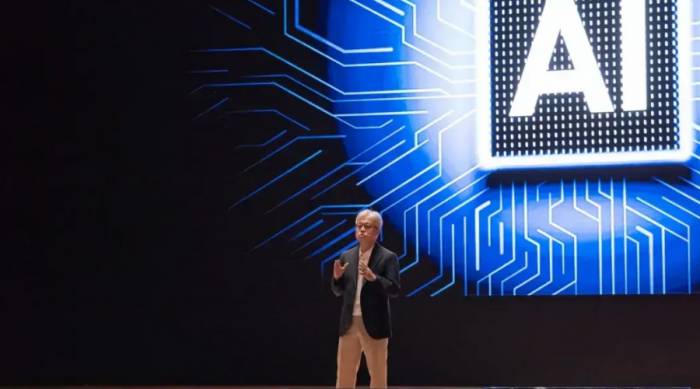
At TSMC's second-quarter legal conference over the past two days, TSMC announced a new concept called "Foundry 2.0."
What is Foundry 2.0? The traditional concept of wafer foundry is usually equated with the manufacturing and processing of wafer products. However, TSMC Chairman Wei Zhejia believes that the 2.0 version of wafer foundry includes packaging, testing, mask making, and other links, excluding the IDM (Integrated Device Manufacturer) of storage chips.
More simply put, everything except chip design can be classified into Foundry 2.0.
TSMC pointed out that the new definition can more fully reflect the continuously expanding future market opportunities. According to the 2.0 definition, the scale of the wafer manufacturing industry reached nearly 250 billion US dollars in 2023, a significant increase compared to the 115 billion US dollars defined by the 1.0 version. It is estimated that the wafer manufacturing industry will grow by nearly 10% year-on-year in 2024.
Data from the research institution TrendForce shows that under the old definition of wafer foundry, TSMC's market share in Q1 reached 61.7%. However, with the new definition, TSMC's total market share in the wafer foundry business in 2023 is 28%.
Advertisement
TSMC's CFO Huang Renshao said that the reason for redefining wafer foundry is due to the entry of international IDM manufacturers into the foundry market, which has gradually blurred the boundaries of wafer foundry. On the other hand, TSMC also needs to continuously expand its own foundry influence, especially in the field of advanced packaging.
However, TSMC also reiterated that it will focus on the most advanced back-end technology to help customers create forward-looking products, which means that the future will still focus on related advanced packaging rather than entering the entire packaging market.
Intel proposed the strategy of IDM 2.0 as early as 2021, separating its foundry department and starting to accept orders from other fabless manufacturers. Now, TSMC's proposal of the Foundry 2.0 concept has a somewhat confrontational feeling. Although TSMC has received orders for Intel's new processors, the two manufacturers are now direct competitors in the foundry market.
Who is the true Foundry 2.0?
Intel's IDM 2.0In 2021, after Pat Gelsinger took over as CEO of Intel, he announced the bold IDM 2.0 plan. He stated that Intel's future goals include becoming a leading semiconductor foundry. At that time, this plan seemed somewhat unrealistic for no other reason than Intel was not only lagging behind TSMC in process nodes but also lost to Samsung.
Intel clearly recognized that its once proud semiconductor process technology could now only be second to others. The backwardness of the process, in turn, affected its own processors. When the traditional PC and server processor market faced fiercer competition, the former giant urgently needed a revolution.
The IDM 2.0 strategy is this revolution, which includes three key components: 1) Expanding Intel's manufacturing capabilities, adopting industry-leading process technologies, 2) Expanding the use of third-party foundry capabilities to meet Intel's internal needs, 3) Becoming a world-class foundry, with the goal of becoming the second-largest foundry by 2030. To achieve these high goals, Intel has committed to delivering five new process nodes in four years to regain leadership in process technology and plans to invest $100 billion to expand capacity by expanding and building six new factories at existing plants in Arizona, Ohio, and Germany.
Firstly, it can be clearly stated that the wafer fab may be the most expensive link in chip production. IDM and Foundry not only need to continuously invest in new manufacturing process technologies to continue to improve semiconductor performance, density, and cost but also need to continuously invest in new manufacturing capabilities. Historically, both of these expenses have been growing exponentially. Intel estimates that switching to extreme ultraviolet lithography (EUV) technology will increase the cost of new factories to about $25 billion, and the next generation of high numerical aperture (High-NA) EUV technology will further increase costs to $30 billion. The high cost has actually excluded manufacturers other than Intel, TSMC, and Samsung.
This is also one of the reasons why Intel is turning to the foundry field. In terms of advanced processes, Intel's competitors are actually only two, and both manufacturers are located in East Asia, with a considerable geographical distance from North American chip design companies. As a domestic manufacturer in the United States, Intel has an innate advantage.
However, this geographical advantage will not directly transform into a competitive advantage in the market. The most critical point of IDM 2.0 is the need for Intel to change its business strategy, from a pure IDM to a Foundry. Samsung and GlobalFoundries have completed this transformation, with GlobalFoundries becoming a pure foundry similar to TSMC, and Samsung splitting into product and foundry service companies, similar to the model that Intel is pursuing.
Intel has also tried to provide foundry services to external manufacturers, but the actual competitiveness is limited. The problem is not only about the price. If you want to use Intel's foundry services, you need to use its proprietary design tools, and Intel is unwilling to modify the manufacturing process for individual products. This basically excludes those applications that are sensitive to cost and power consumption. Under the new strategy, Intel has begun to think and act like a foundry like TSMC.
It has to be said that Intel's measures after the pain have been very effective.
The first transformation is that Intel not only opened its own wafer fab but also opened Intel's packaging services. Intel has long-term R&D investment in advanced packaging and is one of the earliest companies to use multi-chip modules, demonstrating the ability to stack chips through silicon through-silicon vias (TSV) and leading the use of glass substrates for future high-performance applications. In the past, companies wanted to use Intel's expertise in packaging, but Intel rejected these businesses unless all the chips were manufactured at the same time. Opening its advanced packaging capabilities is the initial growth point of Intel's initial foundry revenue under IDM 2.0, accompanied by additional investment in packaging capabilities in existing facilities in New Mexico and Malaysia, especially its embedded multi-chip interconnect (EMIB) and 3D Foveros packaging capabilities, as well as new facilities in Poland.The second transformation is the delivery of new process technologies to restore Intel's competitiveness and ultimately achieve a leading position. To achieve this goal, Intel committed to delivering five new process nodes within four years. At this year's Intel Direct Connect conference, Intel fulfilled this commitment by launching the fifth process node, 18A. In addition, the company also announced the sixth major process node, 14A, and introduced several specialized sub-nodes, which are common in foundries to meet the diverse needs of different products and applications.
Intel further discussed its comparison with other leading foundries in terms of each process node and advanced packaging to demonstrate its current position in the competition and when it will surpass its competitors. According to Intel, the 18A process node will put the company back in a leading position in high-performance computing (HPC) applications, even surpassing competitors in some cases. Intel believes that the 14A generation will also put the company ahead of competitors in mobile applications. Intel plans to restore the normal pace of one process node every two years.
The third transformation is the increase in manufacturing capacity investment and the change in the way investment management is conducted. As governments in various countries want to ensure the supply security and economic growth of the semiconductor manufacturing industry in the future, Intel has made substantial investments in its existing facilities in Oregon, Ireland, and Israel, and has also built six new fabs in Arizona, Ohio, and Germany. Most of the initial investments were made without government subsidy commitments, such as the U.S. chip act. However, Intel has now received more than $50 billion in U.S. and European government incentives, customer commitments (starting with the first five 18A process node customers), and financial partners. Intel has also obtained a $11 billion loan from the U.S. government and a 25% investment tax credit.
In addition to its own capacity investment, Intel has also cooperated with Tower and UMC, two long-standing and successful foundries. Tower will invest in new equipment installed at Intel's New Mexico facility to produce analog products, while UMC will cooperate with Intel to use the three old fabs and process nodes in Arizona, starting from 12nm, to support applications such as industrial IoT, mobile, communication infrastructure, and networking.
The other side of the investment is how to use the current and future capacity. As a pure IDM, Intel has always capitalized on physical facility investment by renovating fabs on average every three process nodes. Although this allows for the reuse of structures and infrastructure, it eliminates support for old process nodes, which is very important for many foundry customers. According to research by Omdia Research, less than 3% of all semiconductors are produced on the latest process nodes. Therefore, Intel is shifting from renovating fabs to support new process nodes to maintaining fabs to support the extended life cycle of old process nodes, as shown in the figure below. This requires additional capacity for new process nodes.
It is worth noting that a fab can support multiple process nodes. Equipment is highly reused between process nodes. The difference lies in the number of steps between one process and another, such as immersion lithography and EUV lithography. However, some process node transitions require higher additional capacity investment, such as the transition to the 14A node, because High-NA lithography technology is introduced. Intel believes that new capital investment will peak by 2024. The result will be lower investment and higher returns starting in 2025, especially as new customers begin to utilize Intel's old process nodes and fully depreciated process nodes.
The fourth transformation, and the most impressive, is Intel's rapid shift to support industry-standard electronic design automation (EDA) tools. As pointed out at the Direct Connect conference, Intel now supports all industry-standard EDA tools from companies such as Ansys, Cadence, Siemens, and Synopsys. This is crucial for simplifying the use of Intel's foundry services. It also overcomes one of the biggest obstacles that other semiconductor suppliers have had in the past for not using Intel as a foundry.
The fifth transformation is the completion of the separation of the wafer manufacturing department, which has now become Intel Foundry. Intel announced a new reporting structure for Intel Foundry this week, including financial restatements dating back to 2021, establishing a unified charging model to serve internal and external customers, and providing revenue and profit forecasts for future Intel products and Intel Foundry Group. Financial data shows that Intel Foundry will continue to lose money in the short term, but Intel believes that by 2030, Intel products (60% gross margin/40% operating profit margin) and Intel Foundry (40% gross margin/30% operating profit margin) will achieve higher profitability.
One advantage for external customers using Intel Foundry is that the process has been fully tested and mass-produced for Intel products. This should significantly reduce the production ramp-up time for external customers. Intel predicts that by 2030, revenue from external customers on advanced packaging, advanced EUV process nodes, and old process nodes will reach $15 billion, and each segment will have strong profit margins. As a result, Intel believes it will return to double-digit investment returns by 2030.
The final transformation is Intel's understanding of being a foundry. Intel is not just providing manufacturing and assembly services for chips for external customers. Intel sees itself as a system foundry, providing a variety of services, leveraging extensive engineering expertise from semiconductor process technology to system development. As Intel CEO Gelsinger said, "The rack is becoming a system, and the system is becoming a chip." As the demand for performance from generative AI workloads continues to increase, the need to put processing, storage, and networking together will become greater. Foreign institutions Tirias Research believe that by 2030, our concept of chips will undergo a huge change. In the highest performance cases, a "chip" may be a single package that requires 2000 watts or more of power. This will completely change the way we think about system architecture.Although the goals of Intel's IDM 2.0 strategy proposed in 2021 are still a long way to go, Intel has fulfilled some of its promises and is on the road to becoming a world-class leading semiconductor foundry service. At present, Intel, which has both advanced processes and advanced packaging, is likely to become one of TSMC's future rivals. TSMC's Foundry 2.0 In the AI wave, Nvidia is the biggest winner, and TSMC, which dominates the manufacturing of data center computing engines, has also made a lot of money. Today, almost all CPUs, GPUs, DPUs, XPUs and FPGAs are produced by this Taiwanese company. In the second quarter of 2024, TSMC's revenue increased by 32.8% to US$20.82 billion, net income increased by 29.2% to US$7.66 billion, and 3nm process revenue reached US$3.12 billion, a year-on-year increase of 83.9%. Specifically in the market segments, HPC business revenue exceeded US$10 billion for the first time, up 57% year-on-year to US$10.83 billion, up 24.7% month-on-month; smartphone business revenue reached US$6.87 billion, up 32.8% year-on-year, but down 4.2% month-on-month; 5nm technology (including N5 and N4 processes) revenue was US$7.29 billion, up 55% year-on-year and 4.4% month-on-month; 7nm revenue fell 1.8% to US$3.54 billion, down 1.3% month-on-month; other old process chip revenue was US$6.87 billion, accounting for one-third of total revenue. From the financial report, it can be found that TSMC's market demand is mainly driven by smartphones and high-performance computing (HPC) businesses. Although the smartphone business experienced a downturn in 2023, it rebounded in 2024, which provided financial support for TSMC's future investment. The growth of the HPC business, especially the demand for AI training and inference chips, has driven TSMC's continued investment and technological innovation in this field. At present, overall, TSMC's investment in AI and HPC is gradually showing results. Although TSMC did not disclose specific AI-related revenue, it is expected to account for at least 9% of total revenue, about US$1.87 billion, and about 17% of HPC revenue. This includes not only the foundry of advanced processes, but also the popular advanced packaging. TSMC plans to further expand CoWoS (silicon interposer integration) packaging capacity in 2026 to meet market demand. From 2023 to 2024, TSMC's CoWoS packaging capacity has doubled and is expected to double again by 2026. Wei Zhejia also elaborated on the new Foundry 2.0 strategy at the meeting. He said: "TSMC's mission is to become a trusted technology and capacity provider for the global logic IC industry. The continued growth in AI demand supports the strong structural demand for energy-efficient computing. As a key enabler of AI applications, customers rely on TSMC to provide the most advanced process and packaging technologies. We use a rigorous framework to respond to long-term market demand, focusing on major industry trends such as AI, HPC and 5G. Our capital investment decisions are based on technology leadership, flexible manufacturing, customer trust and sustainable and healthy returns. To ensure an appropriate return on investment, we are making strategic adjustments in pricing and costs. TSMC is investing heavily in leading professional and advanced packaging technologies to support customer growth and ensure our position as a trusted foundry partner. ” Why TSMC, the leading foundry company, has proposed such a new strategy? Part of the reason may be risk aversion. After all, TSMC's share in the foundry market has reached a monopoly point. The 61.7% share means that all other manufacturers do not make as much as it does. On the other hand, this strategy also expands its growth space. In 2023, the pure foundry market will only be US$115 billion, but the broad foundry market including packaging will be US$247.5 billion. This larger cake also makes it easier for TSMC to "paint the pie": how to continue to increase sales and maintain or even expand profitability in the next few years.As Moore's Law slows down, everything in the semiconductor industry is becoming increasingly expensive, and profitability has always been a challenge. From 2005 to the present, TSMC has been able to bring an average of 35% of its revenue into profit, and from the second half of 2021 to the first half of 2023, TSMC has also achieved a performance beyond the past, with an average profit margin of 41.6%.
However, since the second half of 2023, TSMC's profitability has been on a slight downward trend, and it must look for new profit growth points, which is why we have been hearing rumors that TSMC will increase its manufacturing and packaging service prices.
For TSMC, it is necessary to ensure the advanced process is unimpeded, and to open up the market in advanced packaging. Foundry 2.0 seems to be a slogan shouted by TSMC, but in fact, it is a clear understanding of this foundry - customer-oriented, grasping all the points that can be exerted in the market. The CoWoS packaging can go from concept to landing, also relying on this understanding.
It is interesting to note that TSMC is not the first time to shout the slogan of 2.0. As early as 2000, TSMC launched TSMC-Online 2.0, which was the first personalized Internet information service provided for foundry customers. As a new function for conducting business transactions, TSMC-Online 2.0 has a one-stop wafer service, enabling customers to shorten the actual production time and provide customers with the latest process status control.
What TSMC's next 2.0 is, we are not clear, but for its foundry competitors, Foundry 2.0 is not good news.
Samsung's one-stop foundry
Although Samsung has not thrown out a "XX 2.0" concept like Intel and TSMC, Samsung has already shouted its own slogan for the foundry market.
As early as the SAFE forum held in San Jose in October 2022, MJ Noh, the head of the design service team of Samsung Foundry headquarters, announced the new goals of Samsung Foundry in his speech.
He pointed out that with the development of technology, the "one-size-fits-all" approach is becoming more and more difficult to achieve. Great ideas should not be limited by the pursuit of all-in-one solutions. However, companies need freedom to pursue their own ambitions, so they need a reliable foundry that can provide them with insights and flexibility to meet various needs, even the most unique innovative needs. In a future where cutting-edge technology continues to break through boundaries - from automobiles to mobile devices, from the Internet of Things to high-performance computing and artificial intelligence - is it possible to build a foundry that can unify everything in one place?
Among them, MJ's speech covered how Samsung's advanced design platform uses 2.5D and 3D solutions and other technologies to provide customers with one-stop services that can adapt to the scale and specific requirements of future creative ideas.At the previous forum, Samsung focused on introducing the powerful and extensive capabilities of its design platform across various fields such as automotive, mobile devices, the Internet of Things (IoT), and artificial intelligence (AI), including automotive domain AEC-Q100 certification and ASIL standard readiness. At the same time, the growth rate of high-performance computing applications is particularly fast, and the foundry industry is seeking dynamic modularization of chiplet architecture to find answers. In all these fields, Samsung always focuses on customer priorities when seeking a cooperative platform: accelerating time to market through optimized production cycles and competitive power, performance, and area (PPA) capabilities, such as design technology co-optimization (DTCO) and system technology co-optimization (STCO). Ultimately, the foundry needs to have the ability to provide a one-stop cutting-edge design capability without the need for third-party specialization. Of course, providing all of this is not an easy task.
MJ said: "Traditional chip design methods are facing limitations brought by high costs and integration factors. Even with silicon scaling, the number of transistors is still increasing, pushing the limits of the available maximum photomask size, and the demand for integrating multi-functional chips is rising, which brings serious cost issues in design and manufacturing."
He explained that shrinking transistor sizes will never meet the increasing complexity of applications, which is why Samsung is leading with its continuously advancing 2.5D and 3D chiplet solutions.
More than two years after the one-stop service was proposed, this solution began to shine because of AI.
According to recent reports from South Korean media, Samsung's AI solution strategy based on "one-stop" has begun to attract domestic fabless customers (companies focusing on semiconductor design). Samsung leverages its advantages in memory, foundry (semiconductor foundry production), packaging, and other aspects to provide customized AI one-stop solutions. In particular, by strengthening cooperation with design solution partners (DSPs), it strives to attract potential customers.
On July 9th, Samsung Electronics held the "2024 Samsung Foundry Forum (SFF) and 2024 SAFE (Samsung Advanced Foundry Ecosystem) Forum" in Seoul Coex, and announced the results of strengthening the domestic system semiconductor ecosystem and future support plans.
Samsung Electronics Foundry Business Department Head (President) Choi Si-young said: "As AI's influence on products increases, the number of specialty customers is also increasing. These customers hope to implement various ideas through semiconductors." He explained: "These customers not only need separate design, design assets (IP), processes, packaging, and other solutions, but also need services that integrate the entire system-level verification."
Therefore, Samsung Electronics plans to leverage the advantages of an integrated semiconductor company (IDM) to provide comprehensive AI solution one-stop services that meet customer needs. By strengthening cooperation between the three major business areas of memory, foundry, and packaging, the "lock-in (Lock-In) effect" is maximized to prevent customers from being lost during the product production process. Fabless customers using Samsung's comprehensive AI solutions can reduce semiconductor development and production time by 20%.
In particular, based on the competitiveness of gate-all-around (GAA) process and 2.5D packaging technology, it strengthens advanced process services below 3 nanometers (nm, one billionth of a meter). GAA is a new generation technology that increases the contact surface between the semiconductor's transistor gate (the gate for current entry and exit) and the channel (the path of current flow) to four, which is faster in data processing speed and higher in power efficiency compared to FinFET technology. Samsung Electronics successfully mass-produced the 3nm process applied with GAA for the first time in June 2022 and is currently smoothly advancing the second-generation 3nm process.In addition, Samsung Electronics will actively support outstanding Korean fabless companies in rapidly expanding their influence in the fields of high-performance computing (HPC) and AI. DSP provides design services for semiconductor foundry manufacturing designed by fabless companies. That is, by strengthening the cooperation between "Samsung Foundry-DSP-Fabless," potential customers are attracted.
In cooperation with DSP company Gaon Chips, Samsung Electronics has successfully secured an order for a 2nm (SF2) AI accelerator based on the Preferred Networks (PFN) of Japan, which is a representative achievement of Samsung Electronics' cooperation with domestic DSP. Samsung plans to mass-produce AI accelerator semiconductors for Japan's Preferred Networks based on the 2nm process and 2.5D advanced packaging (I-Cube S).
Furthermore, Samsung Electronics announced that it will expand multi-project wafer (MPW) services to support domestic fabless companies. MPW is a product development method that places multiple project chip designs on a single wafer, mainly used for prototyping or research purposes. Fabless companies do not have their own production lines, so they must prototype through foundries. Through MPW support, Samsung Electronics hopes to attract potential fabless customers in advance.
This year, Samsung Electronics' MPW services have increased by about 10% from last year, totaling 32 times, from the 4nm process to the BCD 130nm process for producing high-performance power semiconductors. It plans to expand to 35 times by 2025. The 4nm process, which is in high demand, will be increased once more this year.
At the event that day, Telechips President Lee Chang-kyu, Above Semiconductor Vice President Park Ho-jin, Rebellions Chief Technology Officer (CTO) Wu Jin-uk, and others served as speakers, sharing the successful cooperation results, vision, and fabless industry trends with Samsung Foundry.
Choi Si-yong emphasized: "Samsung Electronics can integrate memory, foundry, and packaging manufacturing capabilities into one organization, and based on this advantage, we will provide the most effective and optimized solutions for our customers."
Compared with Intel and TSMC, Samsung Foundry has not been eye-catching in the past two years due to repeated setbacks in advanced processes, making its actual performance less dazzling. In front of the two giants who have launched the 2.0 slogan, it seems somewhat overshadowed.
However, Samsung also has its own advantages. After Intel gave up on Optane memory, it is the only foundry company that can provide a one-stop service including memory, manufacturing, and packaging. Facing those small and medium-sized enterprises that are rapidly developing due to AI, it can provide advantages that other companies cannot.
But the downside is that Samsung's current HBM business is not satisfactory. It seems to have become a mediocre player. Although it is not outstanding in all aspects, it still has excellent technical strength. How to make itself stand out in both strengths and weaknesses may be a question that this Korean company needs to consider.
Fierce competition in foundry manufacturingWhether it's TSMC or Intel, or even Samsung, they are all heavily investing in foundry services. Intel plans to increase its capital expenditure by 2% in 2024, reaching $26.2 billion; TSMC's capital expenditure this year is expected to be between $28 billion and $32 billion. Meanwhile, Samsung's capital expenditure for semiconductors in 2023 reached $37.268 billion.
There are also reports that TSMC's capital expenditure this year will reach the upper limit of the estimated range, and next year it is expected to increase by another $5 billion, reaching $37 billion, which is likely to set a historical second high. The huge expenditure makes it difficult for other companies to catch up.
With the slowdown of Moore's Law, the war among the foundry giants seems to have reached a white-hot stage. Endless new strategies and continuous capital output are continuously increasing the intensity of this war. The standard for the final judgment of winners and losers is also very simple: whoever can continue to expand their share in the next few years will be the representative of the future, the real foundry 2.0.
Comments