For a long time, driven by Moore's Law, wafer foundries have been closely pursuing the chip manufacturing process all the way forward. To this day, only TSMC, Samsung, and Intel are left in this final battle, engaging in close combat at the advanced process node.
In recent years, driven by artificial intelligence, mobile, and high-performance computing applications, the semiconductor market has gradually recovered, and the market demand for advanced process capacity is very strong. According to data forecasts, the proportion of global chip manufacturing capacity below 10nm will increase significantly, rising from 16% in 2021 to nearly 30% in 2024.
On the other hand, the competition among the major giants aiming at the advanced process is also very fierce, all intending to gain more market share by demonstrating their comprehensive strength.
In this counterattack and defense battle of the wafer foundry industry, TSMC, Samsung, and Intel are all constantly innovating and competing for the leading position in process technology. Will TSMC continue to "ascend to the throne"? Samsung and Intel, who are attacking on multiple fronts, will they get a few pieces of the pie?
Advertisement
TSMC Discloses Process Roadmap and Prospects
As a leader in the semiconductor industry, TSMC has made great achievements in the past 30 years and has become the world's largest chip foundry.
In the rapid evolution of semiconductor technology, TSMC has always been a leader in global advanced process technology.
TSMC Process Roadmap Disclosure
Recently, TSMC has announced a series of ambitious process roadmap updates, indicating that semiconductor manufacturing is about to enter an unprecedented era—the arrival of the Angstrom process node.
According to its process roadmap, between 2025 and 2026, several key process technologies that TSMC is about to launch, including N3X, N2, N2P, and the revolutionary A16 process, reveal how they will push the boundaries of technology, as well as the impact of these advancements on the performance, energy consumption, and future development of electronic products.TSMC Technology Roadmap
N3P: As an enhanced version of the N3 process, N3P further optimizes performance, power consumption, and density, providing customers with more options.
N3X: A 3-nanometer process designed for ultimate performance, it achieves a 7% power reduction at the same frequency by lowering the voltage to 0.9V, while also enhancing performance by 5% or increasing transistor density by about 10% in the same area.
N2: TSMC's first node to adopt full-gate (GAA) nanosheet transistor technology, GAA transistors enhance current control by surrounding the channel with gate electrodes, thereby significantly improving PPA characteristics. Compared to N3E, N2 shows clear progress, with power consumption reduced by 25%-30%, performance increased by 10%-15%, and transistor density increased by 15%.
N2P: The performance-enhanced version of N2, further optimizing power consumption and performance. With the same number of transistors and frequency, N2P is expected to reduce power consumption by 5%-10% and enhance performance by 5%-10%. It is suitable for applications with high requirements for both aspects.
A16: TSMC's A16 process introduces the backside power delivery network technology (BSPDN) for the first time, integrating the power supply directly into the back of the transistor, greatly improving power transmission efficiency and transistor density. Combined with GAA nanosheet transistors, the goal is to achieve significant improvements in performance and energy efficiency. A16 will become the first "angstrom-level" process node, marking a new era in semiconductor manufacturing.
Compared to N2P, A16 is expected to enhance performance by 8%-10% and reduce power consumption by 15%-20% at the same voltage and complexity, with chip density increased by 1.1 times. The introduction of this technology will open up new possibilities for high-performance computing products, especially those with very high requirements for energy efficiency and signal path.
Overall, this series of technological innovations in TSMC's process technology not only demonstrates its continued leadership in the field of semiconductor manufacturing but also lays a solid foundation for the performance upgrade, energy efficiency improvement, and broader technological innovation of future electronic products. Especially with the arrival of the "angstrom" process node, the semiconductor industry is entering a new era full of challenges and opportunities.Additionally, it is understood that TSMC's A16 process does not rely on the latest High-NA EUV technology, which makes the cost more competitive and meets the urgent need for design optimization by current AI chip companies.
It is also worth noting that TSMC's entire N2 series will add a brand new NanoFlex feature, which allows chip designers to mix and match cells from different libraries in the same design to optimize the chip's performance, power, and area (PPA).
Compared to TSMC's N3 manufacturing process, which already supports similar functions such as FinFlex, the N2 relies on GAAFET transistors, so NanoFlex provides TSMC with some additional control: for example, TSMC can optimize channel width to improve performance and power, and then build short cells (to improve area and power efficiency) or high cells (to increase performance by 15%).
In terms of timing, TSMC's N2 process will enter risk production in 2025 and enter mass production in the second half of 2025; the performance-enhanced N2P and the voltage-enhanced N2X will be introduced in 2026; the A16 advanced process is expected to be launched in the second half of 2026.
TSMC Market Outlook: Strong AI demand, weak automotive and industrial control
According to the recently released revenue ranking of the world's top ten wafer foundries in the first quarter of 2024 by TrendForce, a market research institution, although the demand for AI-related HPC is quite strong, TSMC's first quarter revenue still decreased by about 4.1% quarter-on-quarter to 18.85 billion US dollars due to the off-season of consumer goods such as smartphones and notebooks. Due to the same challenges faced by other competitors during the off-season, the market share remained at 61.7%. In the second quarter, with the main customer Apple entering the procurement cycle and the demand for AI server-related HPC chips remaining stable, there is a chance to drive the revenue to a single-digit quarter growth rate.
Other data shows that in the first five months of 2024, TSMC's revenue increased by 27% year-on-year, far exceeding the industry average, indicating that TSMC's market demand is still strong.
Currently, TSMC occupies 61% of the global foundry market share, far exceeding the 11% of Samsung, which ranks second. This market-leading position makes TSMC very attractive to customers, and many top chip manufacturers, such as Nvidia, AMD, Apple, and Qualcomm, are its long-term partners.With the rapid development of AI technology, the demand for AI chips is experiencing explosive growth. TSMC's Senior Vice President and Deputy Co-Chief Operating Officer in charge of Eurasian business, Yongqing Hou, pointed out that this year's AI demand is very strong, and the mobile phone and PC businesses have also begun to slowly recover, but the demand for automotive and industrial control is still slightly weak.
From the data, compared with last year, the growth of AI accelerators this year is about 2.5 times; the PC market will have a growth of 1-3% this year; after two years of decline, the mobile phone market will grow by 1-3% this year; the automotive chip market demand is weak this year, with an estimated decline of 1-3% in performance; IoT is expected to grow by 7-9%, but compared to the past year's growth of 20%, it is showing a decline.
Citi points out that most AI GPUs currently use 4/5/7-nanometer processes, and as the demand for AI PCs and smartphones grows, coupled with the gradual maturation of chip manufacturing technology, it is expected that most of them will migrate to 3-nanometer processes by the end of 2025. As a leader in advanced semiconductor technology, TSMC is expected to receive more 3-nanometer chip orders in 2025, especially from customers such as Apple, Qualcomm, and MediaTek. At that time, the utilization rate of TSMC's 3-nanometer process will remain tight.
TSMC has also stated that it expects capital expenditure to be between $28 billion and $32 billion in 2024, and it may increase to $35 billion to $40 billion in 2025. These huge budgets are mainly used for the research and development and production of 2/3-nanometer processes.
TSMC has established a solid market foundation through continuous technological innovation and strategic investment.
Global expansion of production capacity, advanced processes remain in Taiwan
TSMC produces most of the world's most advanced processors in Taiwan, but in recent years, it has been changing its strategy, keeping manufacturing operations in Taiwan while building wafer fabs in the United States to produce advanced chips, producing quite advanced processors in Japan, and producing specialized chips in Europe.
It is understood that TSMC has built five new factories from 2022 to 2023, and there are seven factories under construction this year, including three wafer fabs, two packaging factories, and two overseas wafer fabs, with TSMC's advanced process accounting for 67% this year.
In terms of foundry, the new Hsinchu Fab 20 and Kaohsiung Fab 22 built in Taiwan are both 2-nanometer wafer fabs, which have started to be equipped and are expected to be mass-produced in 2025.
Globally, TSMC plans to invest $65 billion in building three cutting-edge process wafer fabs in Arizona, USA. Among them, the first wafer fab has started to be equipped and is expected to be mass-produced in 4nm next year; the second wafer fab, which started construction at the end of 2022, is expected to be mass-produced in 3nm in 2028; the third wafer fab is still in planning, and it is expected to enter mass production before 2030.In Kumamoto, Japan, TSMC plans to build two wafer fabs. The first Kumamoto wafer fab is scheduled to start construction in April 2022, with mass production of 22/28nm and 12/16nm processes expected in the fourth quarter of this year. The second Kumamoto fab is expected to mass produce 6/7nm processes in 2027. In Germany, TSMC will build a 16nm wafer fab, which is expected to start construction in the fourth quarter of this year and mass produce in 2027.
Focusing on advanced packaging, TSMC is also accelerating the expansion of CoWoS and SoIC capacity. According to the plan, the compound annual growth rate of the CoWoS production line will exceed 60% by 2026, and the capacity at the end of the year will be four times that of 2023. The SoIC capacity will increase by eight times compared to 2023, with a compound annual growth rate as high as 100%.
With a multi-pronged approach, TSMC has unveiled its bold roadmap, outlining a grand blueprint in terms of advanced processes, advanced packaging, and international layout. However, it also stated that the most critical development will remain in Taiwan.
In May of this year, Wu Zhengwen, the newly appointed Minister of Science and Technology in Taiwan, expressed his belief that TSMC can protect its proprietary advanced technology and continue to build its cutting-edge wafer fabs in Taiwan while expanding internationally. Although TSMC is developing globally, its most advanced technology development will still be secured in Taiwan.
TSMC: Global Factory Replication Plan
TSMC has also confirmed recently that its overseas wafer fabs replicate the technology and process recipes first adopted in Taiwan. The industry has fully recognized that large multinational wafer fabs need a set of processes to replicate their facilities. As the scale of Gigafab (super wafer fab) expands, in order to maintain the necessary production volume and avoid quarterly bottlenecks caused by the need to readjust the wafer fab, chip manufacturers need to be able to quickly apply new and updated manufacturing processes to other facilities.
Intel is already known for its "exact replication" plan, which allows its wafer fabs around the world to share process recipes, improve production, and reduce performance fluctuations, becoming one of Intel's main competitive advantages.
Similarly, as TSMC continues to add new capacity globally, it has also started to implement a similar plan to quickly improve the production and efficiency of its newly built wafer fabs in Japan and the United States.
It is reported that TSMC has implemented a unified wafer fab management to ensure that super wafer fabs worldwide can achieve consistent operational efficiency and production quality. At the same time, it is also committed to sustainable development in its global business, which covers green manufacturing, global talent cultivation, supply chain localization, and fulfilling social responsibilities.When discussing the improvement of manufacturing technology, there are two main mechanisms: Continuous Process Improvement (CPI) for increasing production, and Statistical Process Control (SPC) for reducing performance variability. To achieve this, TSMC can utilize CPI and SPC to enhance global production and performance by sharing knowledge between different sites through its global Gigafab manufacturing.
TSMC May Initiate a New Round of Price Increases
Recently, several chip manufacturers and wafer foundries have announced price adjustments one after another.
As leading customers (NVIDIA, AMD, Intel, Qualcomm, MediaTek, Apple, and Google) gradually adopt the 3-nanometer process, TSMC's orders are already fully booked until 2026. As a result, TSMC may initiate a new round of price increase negotiations.
At the shareholders' meeting on June 4, Wei Zhejia, the newly appointed chairman of TSMC who has just taken full command, stated that all AI semiconductors are currently produced by TSMC. This implies that there is a thought of raising prices, and the price increase for 3nm foundry services may be more than 5%.
It should be noted that the "involution" of wafer foundries has already shown signs of convergence. Although the price increase of wafer foundries has not yet become a settled fact, the utilization rate of production capacity of major wafer foundries has significantly improved, and many manufacturers have reached full production, with some even exceeding 100% utilization.
In the industry's view, the continuous improvement of the utilization rate of wafer foundry processes and the full production of some foundries will bring price elasticity in the future.
In addition, the AI boom has greatly increased the demand for CoWoS, and the shortage of TSMC's advanced packaging capacity will continue until 2025. It is reported that TSMC's advanced packaging annual price increase next year will be between 10% and 20%.
Under heavy difficulties, how will Samsung Foundry break through?
In the fierce competition of advanced process chips, TSMC is like a steady leader, while Samsung seems to be in heavy difficulties.Especially in the pursuit of breaking through the 3nm process, Samsung Electronics' yield and energy efficiency issues are particularly prominent. However, as global fabless semiconductor companies and tech giants are turning their attention to the 3nm process, the future trend of mainstream technology has become clear. Against this backdrop, TSMC has attracted the favor of many companies with its excellent technical strength. Industry giants such as Nvidia, AMD, Intel, Qualcomm, MediaTek, Apple, and Google have decided to entrust their orders to the world's largest contract chip manufacturer. This decision undoubtedly further widens the gap between TSMC and Samsung Electronics in market share.
Although Samsung once took the lead in the 3nm process field, the reality is quite cruel. According to reports, the prototypes of Samsung Electronics' foundry department are significantly behind TSMC in key indicators, causing it to lose its early advantage in this race. The choices of companies like Google and Qualcomm are a heavy blow to Samsung. After careful consideration, they finally decided to entrust their orders to TSMC, which undoubtedly adds to Samsung's predicament.
According to TrendForce data, in the first quarter of this year, Samsung Electronics' foundry market share has declined, while TSMC's market share has increased. This trend indicates that TSMC's position in the semiconductor foundry field will be more solid in the future, while Samsung needs to make more efforts in technology and market strategy to catch up with the leader.
Samsung Announces Future Process Roadmap
Recently, Samsung announced the latest roadmap of its chip manufacturing process technology at the 2024 Samsung Foundry Forum, involving key points such as 2nm/1.4nm processes and providing a roadmap with back-side power supply technology to customers in the next three years.
Among them, the SF2 node (formerly known as SF3P) is expected to be launched in 2025, mainly designed for high-performance computing and smartphone applications. Compared with the 3nm process (SF3), Samsung's 2nm process has a 12% performance improvement, a 25% power efficiency improvement, and a 5% area reduction.
In 2026, Samsung plans to launch SF2P, which is a performance-enhanced version of SF2, characterized by faster speed but lower density; in 2027, Samsung will release SF2Z, which will adopt back-side power supply technology (BSPDN) to improve performance and increase transistor density. In addition, this improvement also aims to improve power supply quality and manage voltage drop (IR Drop) to address key challenges in the production process of advanced chips.
The Samsung SF1.4 node (1.4 nanometers) plan marks Samsung's hope to enter the 1.4-nanometer race in 2027. Unlike SF2Z, SF1.4 will not include back-side power transfer, which makes Samsung different from Intel and TSMC, which will introduce back-side power supply technology in their 2nm and 1.6nm nodes.
In addition to launching high-end nodes, Samsung also released the SF4U node, which is a cost-effective variant of the 4nm node, improving power, performance, and area through optical shrinkage, and is expected to be mass-produced in 2025.Samsung's latest technology roadmap showcases its continuous innovation and development at the 2nm and below nodes. With the introduction of BSPDN technology and the launch of the 1.4nm node, Samsung is committed to maintaining a leading position in the field of semiconductor manufacturing.
In the past year, Samsung foundry's AI-related sales have grown by 80%, and it is expected that by 2028, the number of its AI chip foundry customers will increase by four times compared to 2023, and the foundry sales will increase by nine times compared to 2023.
Samsung Electronics is developing an AI solution that integrates packaging wafer foundry non-memory semiconductors and HBM, aiming to manufacture AI chips that are both high-performance and low-power. Compared to existing technologies, this new process is expected to shorten the time from R&D to production by about 20%.
Dr. Choi Si-young, President of Samsung Electronics and head of the foundry business, said: "In an era where numerous technologies are developing around artificial intelligence, the key to achieving AI is high-performance, low-power semiconductors. In addition to the mature GAA process optimized for AI chips, we also plan to launch integrated co-packaged optical (CPO) technology to achieve high-speed, low-power data processing, providing customers with a one-stop artificial intelligence solution."
In addition, at the forum, Samsung also shared its plan to adopt silicon photonics in 2027, which is its first announcement of such a plan. Using optical fibers to transmit data on the chip, it is expected that the data transmission speed will be greatly increased compared to I/O.
Samsung wafer factory, another customer loss
As mentioned above, customers have successively decided to place orders with TSMC, which undoubtedly adds to Samsung's predicament.
Recently, it was reported that DeepX, which had previously used Samsung's foundry as a production partner, recently signed an agreement with TSMC's design company partner Asicland, planning to use TSMC's advanced nodes to manufacture SoCs with neural processing units (NPU).
In addition, although there have been rumors for a long time that Samsung provides 3nm process services for AMD, AMD CEO Lisa Su emphasized at the 2024 Taipei International Computer Show that the company is still cooperating with TSMC.It is not difficult to see how difficult it is to snatch advanced process orders from competitors.
In addition to the loss of 3nm customers mentioned above, Samsung's 4nm process has also paid a price.
Qualcomm had entrusted Samsung to manufacture its chips for two consecutive generations, but it is said that Samsung's 4nm process only has a 35% yield rate, which has always been unable to increase production capacity, leading Qualcomm to transfer the order to TSMC to manufacture the Snapdragon 8 Gen 1 Plus chip with 4nm process. Subsequently, from Snapdragon 8+, Snapdragon 8 Gen 2 to Snapdragon 7+ chips, Qualcomm has turned to TSMC.
NVIDIA's RTX 40 graphics card also gave up Samsung and switched to TSMC's 5nm process, and these manufacturers will continue to cooperate with TSMC in the future.
It can be seen that Samsung has paid a painful lesson for its chip process yield rate. Subsequently, its process technology not only needs to keep up with the pace, but Samsung's wafer foundry department also needs to go all out to improve the yield rate, otherwise, the story of being ignored due to low yield rate may be repeated.
Intel foundry, aiming at cutting-edge nodes
The demand for computing power triggered by the new round of AI wave is rapidly expanding. While NVIDIA, the king of GPUs, is worshipped on the altar, Intel, the CPU overlord, seems a bit lonely.
The financial report for the first quarter of 2024 shows that Intel's revenue continues to grow, but the profit has not improved significantly. However, facing competition, Intel still has momentum. From its large bet on AI chips and chip foundry, Intel is finding the lost throne in the new AI era.
From the perspective of foundry business, Intel is also actively promoting the development of its strategic goal of cutting-edge nodes.
Intel recently announced that it has started mass production for customers with the Intel 3 process. Intel 3 represents the third process node in Intel's IDM 2.0 strategy, which aims to develop five process nodes within four years and will become the first advanced node for foundry manufacturing.The Intel 3 process node brings several significant advantages, including a more dense design library, greater transistor driving current, and increased use of EUV (Extreme Ultraviolet) lithography. This node also has three variants, namely 3-T, 3-E, and 3-PT. The first two variants offer an 18% performance improvement per watt compared to Intel 4, while the PT variant brings additional performance and ease of use. All four node variants support a 240nm high-performance and 210nm high-density library. The "T" stands for Through-Silicon Vias (TSVs), which are vertical electrical connections enabling high-speed interconnects between chip components or stacked chips.
From Intel's perspective, the Intel 3 will support foundry customers for at least ten years in the future, opening the door for applications that require a longer lifecycle, such as automotive and IoT. The ramp-up of Intel 3 production is not just a manufacturing achievement; it represents an important milestone and proof point for Intel's foundry business.
It is worth mentioning that the Intel 3 node is the last generation of FinFET nodes on Intel's roadmap, as Intel will start introducing its GAA (Gate-All-Around) transistor RibbonFET from the next generation onwards.
At the earnings call in May, Intel CEO Pat Gelsinger pointed out that the company's first-generation GAA RibbonFET process, namely Intel 20A, is expected to be launched this year; the follow-up product is Intel 18A, which is expected to enter production in the first half of 2025 and gradually progress to the Intel 10A node by 2027.
Intel's two major technologies are RibbonFET and PowerVia: RibbonFET is Intel's implementation of GAA transistors and will be Intel's first new transistor architecture since it pioneered FinFET in 2011; PowerVia is Intel's unique, industry-first backside power delivery network, which optimizes signal transmission by eliminating the need for power wiring on the front side of the wafer.
In Intel's plan, it will also be the first to adopt ASML's latest High-NA EUV lithography machine, which is different from competitors. Intel said that the new tool can significantly improve the resolution and functional expansion capabilities of the next-generation processor, allowing Intel's foundry to continue to lead in process technology after Intel 18A.
At the same time, Intel is also increasing its efforts, announcing the Intel 14A process in February this year, which uses High-NA EUV technology and is expected to be mass-produced as early as 2026. The latest 14A-E version further improves energy efficiency based on 14A.Intel emphasizes the importance of combining with ASML TWINSCAN EXE:5000 High-NA EUV lithography equipment, which will bring new breakthroughs to Intel's process technology and further promote the realization of the process blueprint.
Intel: Striving to become the world's second-largest foundry
Intel's "new process technology roadmap" confirms that its "four years and five process nodes" roadmap is still steadily advancing, and it will be the first in the industry to provide a back-end power supply solution. Intel expects to regain process leadership by 2025 through the Intel 18A process node.
It can be seen that Intel is planning a new path, trying to make itself an important participant in the wafer foundry market, competing with TSMC, Samsung and other wafer foundries, hoping to regain the status of the world's leading chip manufacturer.
Intel's goal is to become the world's second-largest semiconductor manufacturing factory by 2030. To achieve this goal, Intel is strengthening execution and promoting system-level foundry for the AI era, building cutting-edge and diversified manufacturing capabilities.
In addition, Intel also highlighted its progress in mature process nodes, such as the new 12-nanometer node jointly developed with UMC announced in January this year. Intel's foundry plan is to launch a new node every two years and continue to launch evolved versions of the nodes, helping customers continuously improve products with Intel's leading process technology.
Intel Foundry also announced the inclusion of FCBGA 2D+ in the Intel Foundry Advanced System Assembly and Test (Intel Foundry ASAT) technology portfolio, which will include technologies such as FCBGA 2D, FCBGA 2D+, EMIB, Foveros, and Foveros Direct.
Intel Foundry Strategy & Change of Leadership
Since Pat Gelsinger returned to the position of Intel CEO in 2021, the company has actively adjusted its strategy and committed to breaking away from the predicament of traditional products and manufacturing technologies that are difficult to achieve as planned. Under Gelsinger's leadership, Intel, with "IDM2.0" as its core strategy, continues to promote the research and development and implementation of new products and manufacturing technologies.As an important part of the IDM 2.0 strategy, Intel has launched the IFS (Intel Foundry Service) business. Unlike traditional manufacturing models, IFS opens up Intel's manufacturing facilities to other companies besides Intel's product division, undertaking the manufacturing of semiconductor products they design. This innovative model not only expands Intel's business scope but also brings more cooperation opportunities and market space.
The semiconductor industry is known as the representative of "economies of scale," and production scale has an important impact on manufacturing efficiency. At present, manufacturers such as TSMC, which focus on contract manufacturing of high-performance semiconductors, have surpassed Intel's manufacturing division in scale. However, Intel is actively seeking a balance between scale and efficiency through the launch of the IFS business to achieve a larger market share and competitive advantage.
Intel is gradually showing its strong competitiveness and leadership in the semiconductor industry through clear goals, an active roadmap, innovative IDM 2.0 strategy, and the launch of the IFS business.
More than a month ago, Intel announced the appointment of senior industry figure Kevin O'Buckley as Senior Vice President and General Manager of its foundry chip manufacturing business, marking the official launch of Intel's new round of strategic layout in the foundry field. O'Buckley has held senior positions at well-known companies such as IBM, GlobalFoundries, Avera Semiconductor, and Marvell.
O'Buckley's arrival undoubtedly injects new vitality into Intel's foundry business. He will take over from the retiring Stu Pen at the end of May and become a member of the executive leadership team, reporting directly to CEO Pat Gelsinger. This change not only reflects Intel's emphasis on the foundry business but also highlights its deep insight into the development trend of the future semiconductor market.
Intel faces a class-action lawsuit for concealing huge losses.
According to recent foreign media reports, Intel is facing a class-action lawsuit, with investors accusing it of concealing a huge loss of about $7 billion in the "Intel Foundry Service" department.
The report said that investors accused Intel of not correctly disclosing the loss situation of the manufacturing department when reporting the 2023 performance in January this year. The lawsuit alleges that Intel exaggerated the growth and profits of its foundry service department, which actually suffered huge losses in 2023, and the product profits also declined, making the company's positive statements about its foundry strategy misleading, suspected of false statements or concealment.
Not only that, but Intel also outsourced about 30% of its capacity to foundry manufacturers such as TSMC, which further angered investors.The complaint specifically lists the alleged false statements or omissions by Intel, including:
The growth of Intel's foundry services does not represent the growth of reportable revenue within the internal department;
Intel's foundry division suffered significant operational losses in 2023;
Due to a decline in internal revenue, the division's product profit margins have declined;
Therefore, the foundry model will not be a strong driver for the company's Integrated Fulfillment Strategy (IFS);
For the above reasons, the defendants' positive statements about the company's business, operations, and prospects are essentially misleading or lack a reasonable basis.
This lawsuit was initiated by the law firm Levi & Korsinsky, which calls on Intel investors to join the class action lawsuit against the company.
Beyond advanced processes,
The "trio" competes fiercely in advanced packaging
Looking at the roadmaps of the three major foundry giants, the competition in the advanced wafer foundry market is fierce, with TSMC and Samsung competing in advanced processes, and Intel's four-year development of five-node processes is progressing as planned.The three major semiconductor foundry giants are making frequent moves, engaging in a new round of fierce competition.
Data reference: Global Semiconductor Observer
Who will become the next "king" of the wafer foundry industry may still be an open question, but what can be certain is that continuous innovation and technological breakthroughs will be decisive factors.
On the other hand, with the gradual slowdown of Moore's Law, the approach of simply shrinking transistors and increasing density to improve chip performance is failing. In response, advanced packaging has become one of the important solutions to compensate for chip performance and cost in the post-Moore era.
This has also become a new battlefield for the wafer foundry giants.
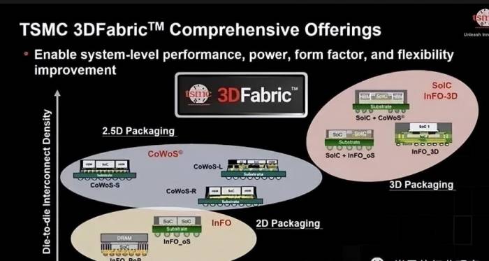
Among them, TSMC is the leader in global advanced packaging technology, with its 3D Fabric offering various advanced packaging processes such as CoWoS, InFO, and SoIC.
CoWoS is one of TSMC's most classic advanced packaging technologies. Since 2011, TSMC's CoWoS process has evolved to its fifth generation, during which the interposer area, the number of transistors, and memory capacity have continuously expanded. Nvidia, AMD, Broadcom, Marvell, and others are major customers of TSMC's CoWoS process.Following the surge in popularity of AIGC, CoWoS has also become a focal point in the industry, with heavyweight clients continuously adding CoWoS orders to TSMC. To meet the needs of major customers, TSMC has accelerated the expansion of its advanced CoWoS packaging capacity.
In addition, TSMC has developed a cost-effective version of CoWoS technology, known as InFO technology, which reduces unit costs and packaging height. This is also an important reason for the success of InFO technology in the mobile application and HPC markets, laying a key foundation for TSMC's later monopoly on Apple's A-series processors.
Apart from CoWoS and InFO, in 2018, TSMC first publicly announced its innovative System-on-Integrated-Circuit (SoIC) multi-chip 3D stacking technology, marking TSMC's capability to directly produce 3D ICs for customers. As the industry's first high-density 3D chiplet stacking technology, SoIC is regarded as the "cutting-edge" technology in 3D packaging.
With its advantages of higher bump density, faster transmission speed, and lower power consumption, SoIC is expected to become the main packaging technology trend for the industry's future development. Currently, TSMC is also actively increasing its SoIC production plan, planning to increase monthly production to 5,000-6,000 units by the end of 2024 to meet the strong demand for AI and HPC in the future.
It is evident that TSMC is reaping the benefits with its leading advanced packaging technology.
Of course, Intel and Samsung, two strong competitors in this field, are also not slacking off.
Intel has introduced various advanced packaging technologies such as EMIB, Foveros, and Co-EMIB through years of technological exploration, continuously refining in terms of interconnect density, power efficiency, and scalability.
From Intel's advanced packaging technology roadmap, it plans to replace traditional substrates with more advanced glass substrates to achieve new breakthroughs; at the same time, Intel will also layout the CPO (Co-Packaged Optics) technology in silicon photonic modules, using the design of glass substrates to increase the available bandwidth during signal exchange through optical transmission, in order to optimize the cost of computing power.
Combining Intel's series of dynamics in advanced processes, the outside world expects that Intel will combine advanced processes with advanced packaging, hoping to achieve a "1 plus 1 greater than 2" effect in the wafer foundry field.Samsung is also actively positioning itself in the field of 2.5D/3D advanced packaging technology and has already launched advanced packaging technologies such as I-Cube and X-Cube. For 2.5D packaging, Samsung's I-Cube technology can compete with TSMC's CoWoS technology. For 3D packaging, Samsung launched the X-Cube technology in 2020, which physically stacks silicon wafers or chips and connects them through TSVs, reducing the interconnect length to the greatest extent, thereby reducing power consumption while improving transmission speed.
In addition, Samsung plans to mass-produce the X-Cube packaging technology, which can handle more data than ordinary bumps, in 2024, and is expected to launch a bumpless packaging technology that can handle more data than X-Cube in 2026. Samsung has the advantage of a comprehensive business portfolio from the design and manufacturing of memory and processor chips to advanced packaging.
In summary, advanced chips are the decisive battle of process technology and also the confrontation of advanced packaging. Advanced packaging and process technology complement each other, playing an important role in the process of improving chip integration, strengthening interconnection, and optimizing performance, and are an important guarantee for the continuous improvement of performance. In the competition for process node time, advanced packaging has become an "indisputable" variable for the three giants.
For more detailed technical details of advanced packaging and the layout of manufacturers, the author has introduced in detail in the previous articles "TSMC's 'Offensive and Defensive War'" and "Advanced Packaging Battle, Upgrade!" For more detailed content, you can refer to the previous articles.
In conclusion, Counterpoint data shows that the semiconductor industry has shown signs of demand recovery in the first quarter of 2024. After several consecutive quarters of destocking, channel inventory has become normalized. The strong demand for AI and the recovery of terminal product demand will become the main growth drivers of the wafer foundry industry in 2024.
With the gradual recovery of the global economy and the increase in semiconductor demand, these will indeed help wafer foundries to seize market opportunities, improve capacity utilization, and enhance cooperation with customers.
However, the semiconductor industry is a highly competitive and rapidly changing field. Wafer foundries need to continuously innovate and adjust strategies to adapt to long-term market changes. In addition, attention should be paid to the stability of the global supply chain, technological progress, and the impact of policy and geopolitical factors.
Looking back at the industry pattern, TSMC's capacity share is more than 60%, but it is still difficult to fully maintain the huge advanced process market. Even if Samsung and Intel's chips will fall into the risk of performance or yield "Waterloo", there will still be manufacturers who are willing to "try the crab" driven by capacity and price factors.In the future, the technological competition centered on advanced processes and advanced packaging will continue for a long time among TSMC, Samsung, and Intel. The tug-of-war among the three giants in the foundry industry will also become the driving force to push Moore's Law to continue moving forward, promoting the arrival of the next "turning point" moment.
Comments