Driven by the surge in generative AI, major chip manufacturers across various industries, including TSMC, Intel, Samsung, SK Hynix, Micron, and ASE, are actively gearing up and expanding their capital expenditures. This is not only a race against time and technology but also a competition of financial resources and strength.
The wafer foundry enters the 2.0 era, where competition among foundries is more intense.
In 2021, Intel proposed the IDM 2.0 strategy, with its core strategy being Intel's Foundry Services (IFS). Around this strategy, Intel made a significant turnaround and made a series of major investments, including building new wafer fabs and upgrading existing facilities.
At the earnings call in the second quarter of 2024, TSMC also proposed the "Wafer Foundry 2.0" concept. According to TSMC Chairman and CEO Mark Liu, they have expanded the original definition of the wafer foundry industry and entered the "Wafer Foundry 2.0" era. Wafer foundry will not only include traditional foundry services but also packaging, testing, mask making, and all IDMs except memory manufacturing. Mark Liu also specifically emphasized that TSMC will focus on the most advanced backend technology, that is, advanced packaging, to help customers achieve leading products.
Advertisement
Both "IDM 2.0" and "Wafer Foundry 2.0" have similar meanings, reflecting the trend of the wafer foundry industry extending to more fields. This also means that more capital expenditures are needed.
According to TrendForce, Intel plans to increase capital expenditures by 2% in 2024, reaching $26.2 billion.
At the earnings call in the second quarter of 2024, TSMC announced that the capital expenditure for 2024 is expected to be between $30 billion and $32 billion, higher than the previously expected lower limit of $28 billion to $32 billion. Among them, 70% to 80% of the capital budget will be used for advanced process technologies, about 10% to 20% for specialized technologies, and about 10% for advanced packaging testing, mask making, and other purposes.
TSMC Chairman Mark Liu said that the main reason for the increase in capital expenditure is the strong structural demand for AI-related growth. In the second quarter of 2024, TSMC's revenue reached $20.8 billion, a sequential increase of 13.6%. Among them, the 3-nanometer process technology contributed 15% of the wafer revenue, while 5-nanometer and 7-nanometer accounted for 35% and 17%, respectively. In terms of platform revenue, high-performance computing (HPC) increased by 28% sequentially, accounting for 52% of the second-quarter revenue, exceeding 50% for the first time. TSMC expects the overall semiconductor market, excluding memory, to grow by about 10% in 2024.
To meet long-term capacity requirements, the TSMC board of directors passed a series of expansion construction resolutions on June 5, 2024, approving a capital allocation of approximately $17.3562 billion for the installation and upgrade of advanced technology capacity, advanced packaging, mature and/or special technology capacity, as well as wafer factory construction and facility system installation.On June 5, 2024, TSMC's board of directors passed a series of decisions on capacity expansion construction. To meet the long-term capacity plan based on market demand forecasts and technology development roadmaps, the board approved capital appropriations of approximately $17.35620 billion for the following purposes: 1) Installation and upgrade of advanced technology capacity; 2) Installation and upgrade of advanced packaging, mature and/or special technology capacity; 3) Wafer factory construction, as well as the installation of wafer factory facility systems.
In view of the continuous investment in 2-nanometer technology, its capital expenditure in 2025 is expected to reach a range of $32 billion to $36 billion, the second highest in history, with an annual increase of 12.5% to 14.3%. The 2-nanometer technology is scheduled to enter mass production in 2025. It is reported that customer demand for TSMC's 2nm process capacity exceeds expectations. In addition to Apple securing the first batch of TSMC's 2nm capacity, non-Apple customers are also actively deploying advanced processes.
In the field of advanced packaging, especially CoWos packaging, TSMC pointed out that the current supply and demand balance has not yet been achieved, and the capacity is continuously increasing. The planned total capacity for 2025 may double. TSMC hopes to achieve balance sometime in 2025 or 2026.
HBM: SK Hynix, Samsung, and Micron are competing fiercely.
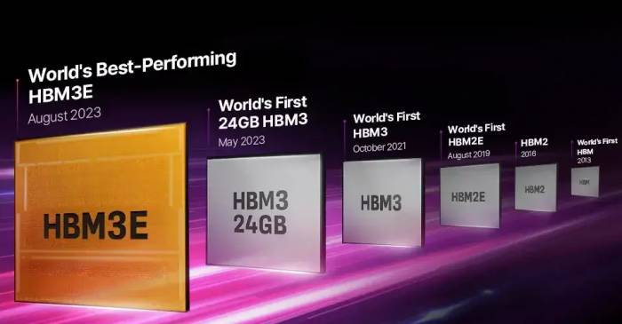
As early as December 2013, SK Hynix released the world's first TSV-based HBM. However, it was not until the explosion of the ChatGPT large language model that HBM was pushed to the forefront of the era. This also made SK Hynix stand out and reach the top of the HBM industry.
Nowadays, the competition in the HBM market is becoming increasingly fierce. In addition to SK Hynix, Samsung and Micron are following closely. With the gradual mass production of HBM3E and the development of the next generation of HBM4, the three giants are in fierce competition. In order to gain an advantage in the upcoming HBM battle, each manufacturer has significantly increased its capital investment.
SK Hynix: $74.8 billion investment in 2028
According to TrendForce's data, the market share of the three major original HBM manufacturers in 2023 is as follows: SK Hynix and Samsung are both around 46-49%, while Micron is about 4-6%. In order to maintain a leading position in the market, SK Hynix is continuously increasing its investment.At the end of June, SK Group, the parent company of SK Hynix, announced in a statement that it plans to invest 103 trillion won (approximately 74.8 billion USD) in SK Hynix by 2028. About 80% of the investment, 82 trillion won, will be used for the development of High Bandwidth Memory (HBM) chips.
SK Hynix has already announced a series of investment plans this year, including the construction of an advanced packaging factory and an artificial intelligence product research center in Indiana, with an investment of 3.87 billion USD. In addition, SK Hynix is currently building the under-construction Cheongju M15X wafer factory, aiming to start mass production in the second half of next year, with an investment of over 20 trillion won (14.6 billion USD). The company also plans to start building the first wafer factory of the Yongin semiconductor cluster next March and complete it as scheduled in May 2027.
In early April this year, SK Hynix also signed an agreement with TSMC to develop and produce the next generation of HBM and enhance the integration of logic and HBM through advanced packaging technology. Through this cooperation, SK Hynix plans to continue developing HBM4 (the sixth generation of the HBM series) and plans to start production in 2026.
Among memory chip manufacturers, SK Hynix is the biggest beneficiary of the explosive growth of AI applications. In the second quarter of 2024, SK Hynix achieved a record high revenue of 16.4233 trillion won, with an operating profit of 5.4685 trillion won and a net profit of 4.12 trillion won. The quarterly operating profit also set a new breakthrough since 2018, breaking through 5 trillion won for the first time in six years, following the semiconductor super boom period in the second quarter of 2018 (5.5739 trillion won) and the third quarter (6.4724 trillion won).
Looking ahead, the proportion of high-value-added products such as HBM3E and server DRAM, which SK Hynix started mass production in March this year, is continuously increasing. The sales volume of HBM increased by more than 80% month-on-month and more than 250% year-on-year, which will continue to drive the company's performance improvement. In addition, SK Hynix predicts that the demand for AI server memory will continue to rise in the second half of the year, and the sales volume of high-performance memory products will also increase with the launch of new PCs and mobile products that support On-Device AI. The company also expects the general memory product market to show a steady growth trend.
Samsung: HBM investment increased by 2.5 times
At the CES2024 at the beginning of this year, Han Jin-man, the head of Samsung's US chip business, said: "Despite the unfavorable market environment, Samsung Electronics has increased the investment in HBM by 2.5 times this year, and will maintain a similar level next year." He also said that this year should be a year to prepare for the demand exceeding supply in 2025.
Among the three companies, Samsung's pace in HBM is slightly slower. In February this year, Samsung announced the development of the industry's first 12-stack HBM3E DRAM HBM3E 12H. According to South Korean media reports, Samsung has reached an agreement with AMD to supply HBM3E worth 4 trillion won (about 2.91 billion USD). On July 24, Reuters reported, citing information from informed sources, that Samsung's HBM3 chips have been approved by Nvidia, but can only be used for less complex H20, which is a customized chip specifically for the Chinese market. In order to speed up the pace in HBM, Samsung has also specially established a new HBM development team, focusing on HBM4.
In terms of investment, Samsung has a larger investment in the United States. The US Department of Commerce (DOC) and Samsung Electronics signed a non-binding preliminary term memorandum (PMT) on April 15, providing up to 6.4 billion USD in direct funding according to the "Chips and Science Act". Samsung is expected to invest more than 40 billion USD in central Texas in the next few years, including HBM and 2.5D packaging capacity.According to reports from the South Korean media outlet, The Korea Economic Daily, Samsung Electronics is planning to apply for a loan of up to 50 trillion won (approximately $3.6 billion) from the Korea Development Bank. This loan is intended for projects to build more chip production facilities both in South Korea and overseas. For many years, Samsung has operated without borrowing, but in the fierce competition of the AI era, Samsung faces strong rivals in the memory and foundry sectors, which may also be a significant reason for Samsung's borrowing. If the agreement is reached, this will be Samsung's first large-scale borrowing in twenty years.
Micron: $30 billion investment by 2030
According to global news media reports from Reuters and Investing.com, Micron's Chief Financial Officer, Matt Murphy, stated on May 21 that the company's capital expenditure forecast for 2024 is expected to reach about $8 billion, higher than the previously estimated $7.5 billion. In the fourth quarter of the fiscal year 2024, Micron will spend about $3 billion on wafer fab construction and new wafer fab equipment (WFE).
This increase is mainly attributed to investment in High Bandwidth Memory (HBM). On February 26, 2024, Micron began mass production of HBM3E. Micron's 24GB 8H HBM3E will be used for Nvidia's H200 Tensor Core GPU, which is expected to start shipping in the second quarter of 2024.
Micron's CEO, Sanjay Mehrotra, indicated in the earnings call on March 20 that the company's HBM (High Bandwidth Memory) capacity has been fully allocated for this year, and most of next year's capacity has also been booked. It is expected that HBM products will bring hundreds of millions of dollars in revenue to Micron in the current fiscal year.
Micron's Chief Operating Officer, Manish Bhatia, stated that the scale of the HBM business is expected to expand to several billion dollars in the fiscal year 2025. In the fiscal year 2025, Micron plans to significantly increase capital expenditure, targeting 30% of revenue, about $12 billion.
From a more long-term investment perspective, Micron plans to invest about $50 billion in total capital expenditure by 2030. On April 25, 2024, Micron received a $6.1 billion CHIPS grant, which will support this $50 billion total expenditure. Micron plans to build a cutting-edge memory manufacturing factory in Boise, Idaho, over the next 20 years, and two cutting-edge memory manufacturing factories in Clay, New York. Micron began construction of the Boise wafer fab in October 2023, which is expected to start construction in 2025 and go into production in 2028.
Yole: About $11.5 billion investment in advanced packaging in 2024
According to BCG analysis, advanced packaging accounts for about 8% of the entire semiconductor market and is expected to double by 2030, reaching over $96 billion, outpacing other parts of the chip industry. Although consumer electronics such as smartphones currently dominate the application of advanced packaging, the booming field of artificial intelligence will drive future growth. Artificial intelligence requires rapid data exchange between computing and memory components, which needs to be achieved through 2.5D and 3D packaging.
Yole intelligence also pointed out that the advanced packaging market is strongly driven by the HPC and generative AI megatrends, and is expected to reach $89.1 billion by 2029. Among all packaging platforms, 2.5D/3D packaging is growing the fastest. The shipment of 2.5D/3D for data center AI processors is expected to grow strongly, with a compound annual growth rate of 23% from 2023 to 2029. Industry giants including TSMC, Intel, Samsung, ASE, Amkor, JCET, and other OSAT manufacturers are heavily investing in high-end advanced packaging capacity, and it is expected to invest about $11.5 billion in their advanced packaging business in 2024.TSMC, Intel, and Samsung have already firmly grasped the high-end packaging market. Traditional OSAT manufacturers must carefully evaluate their best positioning in the market. Although the market is developing, it is to some extent shifting to other parts of the value chain. In the new packaging world, OSAT needs to determine its most advantageous position between simple wire bonding and the most advanced 2.5D/3D packaging.
ASE Technology and TSMC have a close cooperation, and ASE is also a beneficiary of the high demand for CoWoS packaging. It can be seen that this year, ASE has been continuously expanding its investment. Legal persons estimate that ASE's capital expenditure this year could exceed $2.1 billion, and it has the opportunity to reach $2.25 billion.
In February 2024, ASE announced an investment of about NT$2.1 billion (approximately RMB 479 million) to acquire Infineon's two back-end packaging and testing factories in the Philippines and South Korea. ASE Technology's Chief Operating Officer, Wu Tianyu, pointed out at the shareholders' meeting in June that the company has significantly increased its capital expenditure this year, with a larger proportion used for advanced packaging and intelligent production, and continues to invest in smart factories. ASE's Chief Executive Officer, Wu Tianyu, previously stated that the company has increased the expansion of advanced packaging production, and does not rule out establishing more factories in Japan, the United States, or Mexico.
On July 12, ASE Semiconductor's subsidiary, ISE Labs, announced the opening of a second U.S. factory area in San Jose, California. The new ISE Labs factory area was rebuilt to meet the engineering needs of North American customers, serving solution developers in emerging semiconductor application fields such as artificial intelligence/machine learning (AI/ML), advanced driver assistance systems (ADAS), and high-performance computing (HPC).
At present, ISE Labs has one test factory area in Fremont and San Jose. The new San Jose factory is responsible for reliability and verification procedures, while the Fremont factory focuses on testing functions. The total operating space of the two factory areas exceeds 150,000 square feet, making it the largest semiconductor testing service provider in North America.
There are also new players in advanced packaging, such as traditional LCD panel manufacturers, Innolux Display, which is actively transforming and upgrading its production line to an FOPLP advanced packaging production line. According to Innolux Chairman Hong Jinyang, the company's capital expenditure on panel-level fan-out packaging technology in recent years has reached 2 billion yuan. Foxconn's Sharp is also following closely, laying out the FOPLP field. These actions indicate that the competition in the advanced packaging market is becoming increasingly fierce.
In conclusion, no matter what challenges are faced, all industries are accelerating towards the next stage of generative AI. The chip investment war triggered by generative AI is a multi-dimensional, in-depth industrial competition. This global chip investment war will not only promote the advancement of chip technology but also profoundly affect our life and work methods.
Comments