In 2022, SKC's American subsidiary Absolics established its first factory dedicated to the production of glass substrates in Covington, Georgia, with an investment of about 30 billion won (approximately 222 million US dollars). Recently, the company announced the completion of the factory and the start of mass production of prototype products, marking a turning point in the booming market for glass substrates.
The glass substrate market is witnessing fierce competition among major players such as SKC, Samsung Electro-Mechanics, and LG Innotek. Glass substrates are highly valued for their ability to process large amounts of data quickly and their superior energy efficiency compared to traditional plastic substrates. Although the technology is still in its infancy, according to The Insight Partners, the global market size is expected to grow from 23 million US dollars this year to an astonishing 4.2 billion US dollars by 2034.
Currently, the plastic substrate market is mainly dominated by Japan's IBIDEN, Shinko Electric, and Taiwan's Unimicron, but with the increasing performance requirements for semiconductors in the field of artificial intelligence, the shift to glass substrates represents a significant technological advancement.
Why are glass substrates needed?
In the advanced packaging industry, the emergence of glass core substrates has brought the innovation race to a new critical moment.
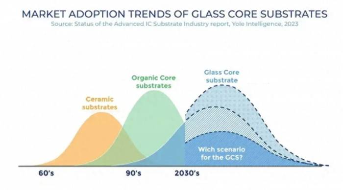
This new technological direction emerged after the wave of organic and ceramic substrates, promising to overcome the challenges of organic core substrates and elevate performance, efficiency, and scalability to new levels in chip design and manufacturing costs, in line with the major trends of HPC and AI. The latter depends on the maturity of the technology and its widespread application in the end market.
Advertisement
As a material, glass has been extensively studied and integrated in various semiconductor industries. It represents a significant advancement in the choice of advanced packaging materials, with multiple advantages compared to organic and ceramic materials. Unlike organic substrates, which have been the mainstream technology for many years, glass has excellent dimensional stability, thermal conductivity, and electrical performance.
However, despite the potential benefits, like any new technology, glass core substrates also face a series of challenges, not only for substrate manufacturers but also for equipment, material, and testing tool suppliers.Despite these challenges, the adoption of glass core substrates is driven by several key factors. The demand for larger substrates and form factors, coupled with the technological trend of chip and heterogeneous integration, is pushing the industry to consider glass as a potential solution. Moreover, once the technology matures and is widely adopted, the potential cost benefits of glass will make it an attractive choice for the high-performance computing (HPC) and data center markets.
In this field, Through Glass Vias (TGV) are one of the pillars of glass core substrates. TGV paves the way for more compact and powerful devices. TGV helps to increase interconnect density between layers. These vias contribute to improving signal integrity in high-speed circuits. The reduction in the distance between connections can reduce signal loss and interference, thereby enhancing overall performance. The integration of TGV can simplify the manufacturing process by eliminating the need for separate interconnect layers. However, despite its many advantages, TGV also faces many challenges. Due to the complexity of the manufacturing process, TGV is more prone to defects that can lead to product failure. In addition, TGV typically means higher production costs than other solutions. The demand for specialized equipment, coupled with the risk of defects, can lead to increased production costs. Recently, many new TGV-related patents have been granted to laser equipment manufacturers such as LPKF. These advancements help to realize the commercialization of glass core substrates while addressing challenges related to glass interposers. This solution can enhance GCS and Glass interposers, bringing hope for exciting next-generation powerful devices.
Furthermore, the synergy between glass core substrates and Panel Level Packaging (PLP) is driving innovation in both fields. As both technologies use similar panel sizes, they provide complementary opportunities to increase chip density, reduce costs, and improve manufacturing efficiency.
Glass core substrates represent a promising frontier in the field of advanced IC substrates and advanced packaging. They offer unparalleled performance and scalability for next-generation chip design and packaging. Although challenges still exist—as with all new technologies—the joint efforts of industry leaders and new entrants are paving the way for the widespread adoption of glass substrates in various end markets, with AI chips and servers being the focus. As GCS technology matures and supply chain infrastructure develops, glass core substrates are expected to redefine the landscape of advanced packaging.
Giant's layout
In September last year, Intel launched a new type of glass substrate technology for system-level packaging chips based on large chips, taking the lead in the glass substrate competition.
Any engineer knows that ICs are not just silicon. Various components (such as packaging, leads, and substrates) affect the durability and ultimate performance of the components. The substrate (the material on which the silicon IC chip is mounted) plays an increasingly important role in achieving higher computing power in a single package. To meet these needs, Intel announced the launch of a new glass substrate technology for the next generation of high-power processors.
Babak Sabi, Senior Vice President and General Manager of Assembly and Test Development at Intel, said: "After ten years of research, Intel has achieved the industry-leading advanced packaging glass substrate. We look forward to launching these cutting-edge technologies to benefit our key players and foundry customers in the next few decades."
According to Intel, compared to today's organic substrates, glass has unique characteristics, such as ultra-low flatness and better thermal and mechanical stability, which greatly improve the interconnect density in the substrate. These advantages will enable chip architects to create high-density, high-performance chip packages for data-intensive workloads such as artificial intelligence (AI). Intel is expected to provide a complete glass substrate solution to the market in the second half of this century, allowing the industry to continue advancing Moore's Law after 2030.
Intel believes that by the end of this century, the semiconductor industry may reach its limits, such as using organic materials to shrink transistors on silicon packaging, which will consume more power and have limitations such as shrinkage and warping. Shrinking transistors is crucial for the progress and development of the semiconductor industry, and glass substrates are a viable and essential next step for the next generation of semiconductors.As the demand for more powerful computing capabilities continues to grow, and the semiconductor industry enters the heterogeneous era of using multiple "chips" in a single package, improvements in signal transmission speed, power transfer, design rules, and the stability of the packaging substrate will be crucial. Compared to the organic substrates used today, glass substrates have excellent mechanical, physical, and optical properties, allowing for more transistors to be connected in a single package, providing better scalability and the ability to assemble larger chip composites (known as "system-in-package"). Chip architects will be able to package more blocks (also known as chips) in a smaller footprint within a package, while achieving performance and density improvements, with greater flexibility and reduced overall cost and power consumption.
In Intel's view, glass substrates will first be introduced to the market where they can be utilized to the greatest extent: applications and workloads that require larger form factor packaging (i.e., data centers, artificial intelligence, graphics) and higher speed capabilities.
Glass substrates can withstand higher temperatures, with a 50% reduction in pattern distortion, have ultra-low flatness, which can improve the depth of focus in lithography, and have the dimensional stability required for extremely tight interlayer interconnect coverage. Due to these unique characteristics, the interconnect density on glass substrates can be increased by 10 times. In addition, the mechanical properties of glass are improved, enabling the packaging of extra-large sizes and achieving a very high assembly yield.
The tolerance of glass substrates to high temperatures also provides flexibility for chip architects, allowing them to flexibly set the design rules for power transfer and signal routing, as it enables them to seamlessly integrate optical interconnects and embed inductors and capacitors into the glass during high-temperature processing. This can achieve better power transfer solutions while achieving the high-speed signal transmission required for low power. These many advantages bring the industry closer to the goal of expanding 1 trillion transistors on packaging by 2030.
As an important player in the industry, Samsung does not want to lag behind.
According to foreign media Sedaily reported in March this year, as one of the world's largest chip manufacturers, Samsung naturally will not ignore glass substrates, so they have recently formed an alliance composed of their own team, aiming to research, develop, and commercialize glass substrates by 2026.
Samsung has formed an alliance composed of Samsung Electro-Mechanics, Samsung Electronics, and Samsung Display to develop and commercialize glass substrates in the shortest possible time. In fact, Samsung Electro-Mechanics announced its plan to mass-produce glass substrates before 2026 at CES.
An industry insider told Sedaily: "Since each company has the world's top technology in their respective markets, the synergy will be maximized in the promising field of glass substrate research, and it is also necessary to pay attention to how the Samsung alliance's glass substrate ecosystem will be established."
Samsung Electronics is expected to focus on the integration of semiconductors and substrates, while Samsung Display will focus on glass processing. This cooperation aims to enhance the competitive advantage of the group.
Subsequently, foreign media ETNews reported in May that Samsung Electro-Mechanics is accelerating its entry into the semiconductor glass substrate market, advancing equipment procurement and installation to September, and starting the trial production line in the fourth quarter, one quarter earlier than the original plan. The company is expected to start producing glass substrates for high-end system-in-package (SiP) in 2026. To secure orders for 2026, the company needs to demonstrate good capabilities in 2025.In order to construct highly complex multi-chip SiPs, Samsung needed to acquire expertise in glass substrates. Therefore, the company's decision to advance the trial production line schedule at its Sejong factory in Korea may be a strategic move, reflecting the growing importance of advanced chip packaging technology to Samsung, as well as the company's active attempt to seize market share from Intel, which is expected to start offering advanced glass substrate packaging in the coming years.
It is reported that Samsung Electro-Mechanics plans to install all necessary equipment on the trial production line before September and start operations in the fourth quarter.
The selection of suppliers has been completed, with companies such as Philoptics, Chemtronics, Joongwoo M-Tech, and German LPKF responsible for providing components for the device. Reports indicate that the device is designed to simplify production and adhere to Samsung's strict safety and automation standards.
As Samsung's foundry attempts to secure more orders from data center processor developers, the company also needs to provide advanced packaging services. Therefore, Samsung Electro-Mechanics' (and in fact, Samsung as a whole) efforts related to glass substrates may soon be crucial to Samsung's foundry business.
LG Innotek has also entered the development of glass substrates. The CTO department of LG Innotek's core R&D division recently began recruiting personnel to develop semiconductor glass substrates. Previously, LG Innotek CEO Hyuk-soo Moon stated at the company's shareholder meeting in March, "Large American semiconductor companies are interested in glass substrates," and "LG Innotek is also preparing for the glass substrate business."
Furthermore, the emergence of new companies such as SCHMID, as well as the participation of laser equipment suppliers, display manufacturers, and chemical suppliers, highlights the diverse ecosystem forming around the emerging supply chain of glass core substrates. All parties are establishing cooperation and partnerships to address the technical and logistical challenges associated with glass substrate manufacturing, indicating that all parties are working together to maximize their potential.
In conclusion, while major manufacturers are vigorously advancing, downstream customers have also expressed enthusiasm for the adoption of glass substrates. Intel goes without saying, and others such as Nvidia, AMD, and Apple are also considered potential "buyers" of glass substrates.
However, despite its many advantages, there are still many factors to be resolved in order to fully commercialize glass substrates. The biggest issue is fragility. The industry believes that achieving mass production yield before actual delivery will take some time. The company's upfront investment cost is also high. Even if the company invests heavily in technology development, if the business is not profitable, it will become a sunk cost.
Hl Investment & Securities researcher Ko Eui-young said, "The glass substrate requires a supply chain reorganization because equipment replacement is needed, and further verification of reliability related to glass materials is required." "Standardization of mass production is a must, but the yield at the time of mass production is uncertain." But in the long run, the industry consensus is that glass substrates should be developed.NH Investment & Securities researcher Lee Kyu-ha said, "In order to optimize the trend of semiconductor miniaturization, glass will become the core of future substrate materials."
Comments