Earlier, Samsung held a foundry forum.
For Samsung, the key to holding such events is to readjust the industry's expectations of the company's competitiveness and production capacity. It is hard not to notice that when partners choose competitors for their latest and most outstanding AI chips, Samsung hopes to gain support from a multitude of high-performance designs such as AI startups, automotive customers, and smartphones, and the company has a solid foundation in a large number of traditional process nodes that are crucial for power, high voltage, and RF solutions.
The focus of Samsung's release at this event is the roadmap of its SF2Z process node. "SF" stands for Samsung Foundry, "2" represents the 2-nanometer level, and Z represents back-side power supply. SF2Z will be the node that integrates the Gate-All-Around technology of this generation (which Samsung calls MBCFET), followed by BSPDN, to improve performance and energy efficiency.
In this article, we will delve into some details, but the key date here is 2027 - Samsung is expected to start mass production at SF2Z. This will be after the company has mass-produced many other SF2-level nodes. SF1.4, an earlier node, will also start risk production in 2027.
Advertisement
Samsung Foundry: Expansion
Given that CHIPS Act funds will flow to Samsung, it is crucial to determine the location of Samsung's facilities. Most of Samsung's traditional and cutting-edge technologies are located in South Korea, distributed across three cities:
Giheung, Line 6, 65nm-350nm: Sensors, Power ICs
Giheung, S1 Line, 8nm: Smartphones, Data Centers, Automotive
Hwaseong, S3 Line, 3nm-10nm
Pyeongtaek S5 Line Phase 1 + Phase 2The third phase of the construction of the Pungze S5 line is underway.
Samsung also has two factories in the United States:
Austin (Texas), S2 line, 14nm-65nm: smartphones, data centers, automotive
Taylor (Texas), announced the construction of 4 new wafer fabs, capable of accommodating 10. It will include SF2, SF4, FDSOI, packaging
Samsung's current packaging facilities are located in South Korea, but it also has a huge influence on global OSAT partners. The expansion plan in Taylor will be the company's largest expansion outside of South Korea, and it plans to provide on-site comprehensive operations for any American company without the need for Asia.
Manufacturing Technology Roadmap
Like other foundries, Samsung relies on a series of main series process nodes, from which many variants are derived. In this case, the main nodes are SF4 and SF2.
SF4 series: FinFET
2021: SF4E (E = Early)
2022: SF42023 Year: SF4P (P = Performance, for Smartphone)
2024 Year: SF4X (X = Extreme, for HPC/AI)
2025 Year: SF4A, SF4U (Automotive, U = Ultr)
Samsung's SF4 remains a FinFET node, which has proven to be very popular in the smartphone chipset market and among a large number of AI startups that want cutting-edge technology. SF4P is primarily targeted at the smartphone sector, with lower leakage than SF4, while SF4X is the product that most AI and HPC users will ultimately choose. For anyone looking for a mid-range GPU in 2024/2025, if they are manufactured by Samsung, then SF4X is your best choice.
Due to the higher requirements of the automotive node, Samsung usually launches a dedicated version of its technology for automotive use, which is where SF4A comes in. SF4U, although called Ultra, is designed to be a higher-value version of SF4P, showcasing a more high-end strategy for smartphone chipset manufacturers who want to benefit from node improvements, but at the same time have a slightly larger margin and effective production.
SF2 Series: MCBFET (GAA)
2022 Year: SF3E
2024 Year: SF3
2025 Year: SF22026: SF2P, SF2X
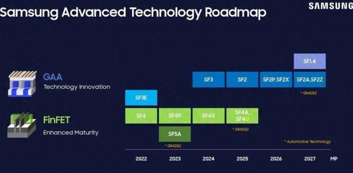
2027: SF2A, SF2Z
So this might be a bit confusing. Samsung's foundry announced that it is the first to produce GAA technology with the SF3E node—appropriately named "early." As far as we know, although mass production has been in place since 2022, it is purely an internal node designed to help develop the technology. Intel will not launch GAA until the 20A/18A node in 2025, and TSMC is also considering launching N2 in a similar timeframe. Both companies hope to quickly bring it to market, rather than making announcements ahead of time like Samsung.
SF3 is the second generation of GAA and has been in mass production since 2024. There might be a rebound, but the third generation, SF2, will be heavily promoted to customers. Users who follow Samsung may notice that the transition from SF3 to SF2 in the naming scheme is a bit strange - this actually means that Samsung has renamed its SF3P and later series to SF2, which may better align with the naming used by Samsung's competitors. The focus of the debate, as always, is competitive alignment, but real customers do know the performance, regardless of the node name.
In 2026, we will see mass production of smartphones (SF2P) and the AI/HPC variant of GAA (SF2X), where we will follow the strategy of the SF4 series very closely. In 2027, we will get the automotive variant, but SF2Z will bring BSPDN to the negotiating table. From the discussions at the event, 2027 is an ideal mass production date for SF2Z, not just a risk production date. This means that risk production of SF2Z will start at the end of 2026 or the beginning of 2027, first in South Korea, and then in the United States at the appropriate time.
It is worth noting that Samsung expects the pace of GAA power improvement to be faster than that of FinFET - a slide shows the trend of planar transistor power (before 14nm) at 0.8 times per year, while the trend during the FinFET period is 0.85 times/year. Samsung expects GAA to restore these improvements to 0.8 times per year through GAA/MCBFET.
Memory Roadmap
Samsung is eager to emphasize its position in the memory ecosystem - mainly as the top supplier. The company has shown that it has been in the first place in DRAM since 1992, with a current market share of 41%; it has been in the first place in NAND since 2002, with a current market share of 32%; and it has been in the first place in SSD since 2006, with a current market share of 37%. Samsung sees the market as a pyramid.
Tier 1: SRAMTier 2: LLC
Tier 3: HBM3E / HBM4
Tier 4: LPDDR6 / LPDDR5X-PIM / LPCAMM
Tier 5: CMM-D (C)
Tier 6: PBSD / CXL-H (C)
I find this inherently interesting because it showcases some of the upcoming technologies that Samsung is researching. We know that memory standards improve over time, such as from HBM3 to HBM4, or from LPDDR5 to LPDDR6, but here it shows that Samsung is achieving memory processing through its LPDDR5X product line. Memory processing is something that Samsung has been talking about for years, initially focusing on the HBM stack and working in conjunction with AMD Xilinx FPGA or custom chip configurations. The fact that it is about to appear on a variant of LPDDR5X is significant, especially if it means power savings in the medium to long term are beneficial for AI. Also on the fourth tier is LPCAMM. The last two tiers are about memory and storage expansion, especially the upcoming CXL standard.
However, the focus of most people is on the HBM aspect. Samsung has revealed some data and timelines:
2022: 8-Hi stack HBM3, with speeds up to 900 GB/second
2024: 12-Hi stack HBM3E, with speeds of 1178 GB/second
2026: 16-Hi stack HBM4, with speeds of 2048 GB/second2028: HBM4E
Regarding HBM4, Samsung has also revealed a lot of information.
Chip Density: 24 GB
Capacity: 48GB/cube
Data Width: 2048 bits (higher than 1024 bits)
Pin Speed: 6 Gbps/pin (lower than 8 Gbps/pin)
Stack Height: 720 micrometers (unchanged)
Bonding: Copper-Copper Hybrid Bonding (updated from previous methods)
Base Chip: Includes buffer, transition from planar FET to FinFET
Samsung lists HBM4 as providing 200% of the speed with 70% of the area and half the power. But that's not the end of the story, as Samsung hopes to customize HBM to become the standard for the highest performance hardware. This means the base chip, which includes logic and buffers, will be individually configured by customers according to their performance profile requirements. This means the same HBM4 can be optimized for reading, or support more memory encryption modes. Combined with more cutting-edge base chips, the goal is to extract performance and improve efficiency, which are two hallmarks of the AI crowd that will use HBM4 in an unparalleled way.Packaging
From my past perspective, at least, one of the areas where Samsung has not been heavily promoting is the packaging business. While other foundries are promoting CoWoS and EMIB/Foveros, it is difficult to say what Samsung's packaging capabilities are, even without a marketing name to summarize. Nevertheless, Samsung is indeed involved in advanced packaging, both for smartphones and AI accelerators.
In the field of smartphones, the roadmap is shown below, listing their respective thermal resistance ratios:
2016: I-POP, 1x TR
2018: FOPLP, TR is 0.85 times
2023: FOWLOP, 0.85 times TR
2025: FOPKG-SIP, 0.65 times TR
In the field of artificial intelligence, Samsung has set the following roadmap for AI chips.
Currently: 2.5D interposer, 6 HBM3, 80 GB capacity, bandwidth of 3.35 TB/s2024: 2.5D interposer+, eight HBM3E, 192 GB capacity, bandwidth of 6.6 TB/s
2026: 2.xD with RDL+Si Bridges, 8-12 HBM4, 576 GB capacity, bandwidth of 30.7 TB/s
2027: 2.xD+3D, logic/logic and logic/memory. 16-24 HBM4E, bandwidth of 70.5 TB/s
The last one did not list the capacity, but we are talking about combining 2.5D and 3D functionalities - essentially integrating multiple AI accelerators together. If the base design has a computing chip and four HBM3E stacks, this can be seen as similar to Blackwell. But Samsung's idea is similar to putting two Blackwells together. Of course, the power consumption of these ASICs is not mentioned!
In terms of 3D integration, we do have some roadmap on when Samsung will offer different bottom chip/top chip support.
Bottom Die: SF4X to be launched in 2025, SF2P in 2027
Top Die: SF2 to be launched in 2025, SF1.4 in 2027
This seems to be a statement of computation on computation, rather than computation on cache or cache on computation.
Samsung also mentioned co-packaged optics (CPO). The company is investing in the CPO strategy, including electrical interface chips (EIC), photonics interface chips (PIC), and optical boards for fast data transfer.
Outside of the presentation, I had a conversation with a photonics engineer from Samsung, and we discussed silicon waveguides as a long-term solution for integrating a large number of chips together - if you are familiar with the startup Lightmatter's Passage, it allows multiple chips to communicate with each other through the package via light, and we discussed that this is a potential future for this technology. Today, most CPO solutions are using GlobalFoundries' 45nm photonic process or imec's 200nm variant - so it is exciting to see competition in this field. Samsung stated that they expect to have EIC/PIC proof of concept soon.Final Thoughts
The roadmap indicates that Samsung is committed to maintaining its leading position in the long term. Being first is one thing, but doing well is another. Samsung boasts a robust local chip design industry—my list includes at least six AI startups, and I am aware that many medium-sized AI hardware companies will utilize SF4X, including Tenstorrent and Groq.
In addition to this, determining the direction of the advanced packaging market is an added benefit, and I hope to see more public discussions and examples of Samsung's capabilities. The forum is a good start, and I look forward to seeing more data.
Comments