Introduction: For at least a decade, the end of Moore's Law has been a topic of discussion. Particularly, the remarks made by two giants in the semiconductor field, Huang Renxun and Kissinger, have left industry veterans and observers puzzled. In 1965, Intel co-founder Gordon Moore predicted that the number of transistors on a single chip would double approximately every two years, with only a minimal increase in cost. This prediction was revolutionary at the time because it foretold an era of continuous innovation and technological advancement. It later became known as "Moore's Law," serving as a guiding compass and beacon for the development of the semiconductor industry, profoundly influencing its growth.
Sixty years of change, Moore's Law leads industry development
Over the past nearly sixty years, Moore's Law has been the beacon of the semiconductor industry, guiding the direction of technological progress. The impact of Moore's Law is profound. From the initial few dozen transistors to today's billions of transistors, Moore's Law has inspired countless technological breakthroughs, including the development of microprocessors, the advancement of memory, and the transformation of the entire electronics industry.
Advertisement
In the 1970s, the Intel 8086 microprocessor accelerated the arrival of the personal computing era. In the 1980s, the first x86 processor with one million transistors was born. In the 1990s, the Intel Pentium processor was born, and the Xeon processor brought powerful computing power to servers and workstations. In the 2000s, the first Intel "Core" with a dual-core structure integrated on a single chip, specifically designed for personal computers, was born.
On the path of transistor miniaturization, challenges have never ceased. However, each time, under the guidance of Moore's Law, the semiconductor industry has successfully overcome numerous difficulties and achieved technological breakthroughs. From strained silicon, Hi-K metal gates to FinFET transistors, semiconductor giants represented by Intel have achieved a series of milestone innovations in the field of transistor miniaturization. Moore's Law has been proven correct time and time again; these innovations have not only greatly improved chip performance but also laid a solid foundation for the continuation of Moore's Law.
Today's world has an exponential demand for computing power. People are eager for more powerful computing capabilities to meet the complex needs of applications such as video, gaming, and artificial intelligence. This demand is inversely proportional to the area, cost, and power consumption of chips. In short, this is "Moore's Law": more abundant, more powerful, and more cost-effective computing power is a key component of economic growth.
Indeed, Moore's Law has achieved tremendous success over the past sixty years, but it also faces some challenges today. As transistor sizes continue to shrink, physical limits are gradually being approached, and the traditional Moore's Law scaling (miniaturization) speed is slowing down. However, this does not mean the end of Moore's Law; instead, it encourages the entire industry to continuously seek new materials, new design architectures, and new manufacturing processes. After all, adversity is the mother of invention.
Moving towards trillions of transistors, how to continue Moore's Law?
As the "golden rule" of semiconductor technology, Moore's Law has laid the foundation for the increasingly digital and intelligent world we live in. The next step is for Moore's Law to continue guiding the development direction of the semiconductor industry.Currently, there are about a billion transistors in a single device, and Intel predicts that by 2030, the number of integrated transistors in a single device will reach one trillion. How can one trillion transistors be achieved? This will be a process of integrating the greatest achievements.
(I) Process Miniaturization: The Eternal Pursuit of Moore's Law
Firstly, the process still needs to continue to be miniaturized, and process miniaturization is the key means to achieve an increase in the number of transistors. As the proposer and practitioner of "Moore's Law," in 2021, Intel proposed a 4-year plan with 5 nodes, leading the semiconductor industry into the era of angstroms. Now, Intel's "four-year five process nodes" plan is proceeding smoothly according to plan.
In the next three important nodes of Intel 20A, Intel 18A, and Intel 14A, Intel will introduce more new technologies. For example, Intel will start using a brand-new transistor architecture - RibbonFET all-around gate (GAA) transistor from Intel 20A. In RibbonFET transistors, the gate can better control the flow of current, while providing stronger driving current at any voltage, making the transistor switch faster, thereby improving the performance of the transistor. The horizontal channel of the RibbonFET transistor architecture can be vertically stacked, instead of placing the fins side by side like FinFET, so it can achieve the same performance with a smaller space, thus promoting further miniaturization of the transistor size. RibbonFET will also further enhance the flexibility of chip design, and its channels can be widened or narrowed according to needs, making it more adaptable to different application scenarios.
PowerVia back-side power supply is another key technology. In the traditional transistor architecture, power lines and signal lines share the same wafer space, limiting the improvement of chip performance and energy efficiency. The back-side power supply technology moves the power lines to the back of the transistor, effectively solving this problem and significantly improving chip performance and energy efficiency. Test results show that chips using PowerVia technology have a standard cell utilization rate of over 90% in most areas, with a significant increase in cell density, and costs are expected to be reduced. At the same time, PowerVia technology has reduced the platform voltage by 30% and achieved a 6% frequency increase. Back-side power supply technology provides important support for transistor miniaturization.
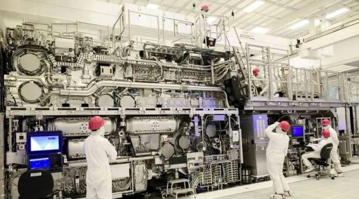
Under the miniaturization of Moore's Law, lithography technology will continue to play an important role. The next generation of EUV lithography technology, High NA EUV, is expected to further enhance the miniaturization capability of transistors. The High NA EUV lithography machine is expected to print features that are 1.7 times smaller than the existing EUV tools. Compared with 0.33NA EUV, High NA EUV (or 0.55NA EUV) can provide higher imaging contrast under similar features, thus requiring less light for each exposure, reducing the time required to print each layer, and increasing wafer yield. Currently, Intel is the first foundry in the industry to receive and assemble the first High NA EUV lithography system in the industry. Intel plans to use high numerical aperture (High NA) extreme ultraviolet (EUV) lithography technology at the Intel 14A node.
(II) Advanced Packaging, Increasingly Important
In recent years, the development and progress of advanced packaging technologies such as 2.5D and 3D have provided a new path for the continuation of Moore's Law and have become the focus of competition among major wafer factories. At present, Intel's advanced packaging technology mainly includes the following aspects:EMIB (Embedded Multi-die Interconnect Bridge) 2.5D Advanced Packaging Technology: Supports interconnecting different chips on the same plane, reducing the bump pitch of chip interconnections to 45 micrometers, significantly increasing chip interconnection density and bandwidth.
Foveros 3D Advanced Packaging Technology: Supports stacking independent chip modules on a vertical plane and achieving vertical interconnections through through-silicon via (TSV) technology, further enhancing transistor density and performance.
Next-generation Foveros technology, Foveros Direct: Adopts a hybrid bonding connection technology of copper to copper instead of soldering, further reducing the bump pitch to below 10 micrometers, and significantly increasing chip interconnection density and bandwidth, as well as reducing resistance.
In addition to innovations in structure and interconnection, material innovation has become indispensable. Industry forecasts suggest that by the end of the 2020s, the semiconductor industry's ability to scale transistors in silicon packaging using organic materials may reach its limits. Organic materials have higher power consumption and are prone to shrinkage and warping during the scaling process. Companies like Intel have begun to explore the potential of glass substrates.
Glass substrates have ultra-low planarity, better thermal stability, and mechanical stability, giving them unique advantages in supporting high-density, high-performance chip packaging. As organic substrates gradually reach their limits in the scaling process, the application of glass substrates will become key to the development of next-generation semiconductor technology.
(III) Beyond Moore's Law
To achieve the goal of integrating one trillion transistors in a single device by 2030, Intel's component research team is also conducting extensive research in several areas, including 3D stacking of CMOS transistors, successfully integrating silicon transistors and gallium nitride (GaN) transistors on the same 300mm wafer, using 2D channel materials such as transition metal dichalcogenides (TMDs), and stacked ferroelectric capacitors. Through continuous innovation in multiple cutting-edge technology fields, Intel's component research team is striving to extend Moore's Law.
"Do not be bound by history, but create brilliance with bold actions," a quote from Intel co-founder Robert Noyce. Looking ahead, although traditional silicon-based processes face bottlenecks, emerging technologies such as quantum computing, photonic computing, and carbon nanotubes are expected to take over the baton of Moore's Law and continue to drive leaps in computing power.
By focusing on both process and packaging, and combining multiple niche technologies, Intel aims to be at the forefront of process technology by 2025. Intel's innovative practices demonstrate its firm determination to surpass Moore's Law and its mission to lead the future development of computing. The goal of one trillion transistors is within reach.
ConclusionGordon Moore wrote in 1995: "I do not expect this estimate to be very precise. I just want to make it clear to everyone that this is a promising technology, and in the long run, it is expected to make a huge contribution." Ultimately, Moore's Law has never been a "law" from the beginning; it is Gordon Moore's observation of semiconductor technology and a prediction of future development.
Over the past half-century, Moore's Law has long been more than just a technical prediction; it has become a spiritual symbol of the semiconductor industry's pursuit of progress. Continuous innovation is the cornerstone of Moore's Law. From the development of silicon transistors to nanometer processes, and now to the exploration of quantum computing and other cutting-edge technologies, Moore's Law has always been pushing the boundaries of technology. It inspires countless scientists and engineers to constantly break through themselves and pursue higher goals.
As Intel CEO Pat Gelsinger said: "Moore's Law will not stop until the periodic table is exhausted." Therefore, as long as innovation continues, Moore's Law will not stop.
Comments