The development of NAND seems to have entered a strange loop.
The former Toshiba Memory, now Kioxia, has just announced good news: with the recovery of the storage market, Kioxia has ended its NAND flash memory production reduction strategy. Currently, the utilization rate of production lines at Kioxia's two factories in Shiga Prefecture's Yotsukaichi and Iwate Prefecture's Kitakami has been increased to 100%.
In addition, after six consecutive quarters of losses, Kioxia has also achieved a profit of 10.3 billion yen in the last quarter. A loan consortium composed of three banks has agreed to refinance Kioxia's upcoming 540 billion yen (currently about 24.925 billion yuan) loan and provide a new credit line of 210 billion yen.
Other storage manufacturers are also striving to restore the previously reduced NAND production capacity. Samsung's NAND flash memory production capacity has climbed to about 70%, SK Hynix is increasing the production of high-capacity NAND products (such as high-capacity eSSDs), and Western Digital is raising its production utilization rate to about 90%.
However, the winter of the NAND market may not have ended yet. Some experts worry that the rapid growth in production may exceed demand, thereby suppressing the rise in NAND flash memory prices. Kim Yang, a researcher at the Korea Institute for Industrial Economics and Trade, said: "Apart from the high-capacity NAND used in artificial intelligence data centers, it is hard to say that the entire NAND market is recovering. The sudden surge in production may lower the NAND prices that have been rising."
Advertisement
This also means that in the coming year, the NAND market still has many uncertainties. Whether it can recover as quickly as DRAM is still unknown.
The greater challenge remains on the technical side: what is the next step for 3D NAND?
For NAND, the first decade of the 21st century was no different from DRAM. With the continuous development of Moore's Law, through higher resolution lithography, the continuous miniaturization of transistors has brought about an increase in storage density and performance.
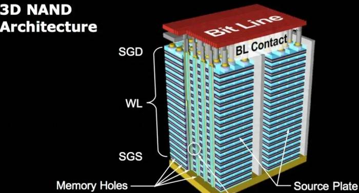
However, after 2010, this path of miniaturization gradually came to an end. On the one hand, the mass production of EUV technology was slower than expected, and DUV had reached its limit. The high cost and low yield of the curve-saving multiple exposure method were also unacceptable to NAND manufacturers.Ultimately, 3D NAND technology has become the new direction for development. Traditional NAND Flash adopts a flat design, while 3D NAND is stacked from the originally laid-out storage cells, increasing from a traditional single layer to a stack of up to hundreds of layers, significantly enhancing its storage capacity compared to traditional 2D NAND Flash.
To this day, 3D NAND continues to drive the development of the entire storage market. However, the debate within the industry about the future direction of NAND seems never to have ceased.
As early as the 2004 International Solid-State Circuits Conference (ISSCC), Jagdish Pathak of Sub-Micron Circuits stated, "In-depth research is needed to continue scaling flash memory technology after 2010. 90-nanometer flash memory is already in production, and there is controversy over 65 nanometers, with some believing it can continue to scale, while others express doubt. I think that when approaching 45 nanometers, the floating gate structure will face greater scaling difficulties. There are many, many challenges."
Dr. Kim Ki-Nam, Vice President of Samsung's memory division, chose a method based on chalcogenide materials (i.e., PCRAM, PRAM, and Ovonics unified memory), which relies on the phase change effect of materials to achieve switching. Kim said, "It has better scalability than other methods."
Tomoyuki Ishii of Hitachi Central Research Laboratory is researching NanoCrystal memory technology, a derivative of single-electron memory technology. Ishii said, "It can scale vertically and horizontally, and multi-state data provides the lowest cost per bit of all alternatives. Oxides can be scaled to a thickness of 5 nanometers, and this is also a pure silicon process." The challenge of NanoCrystal is slow programming and erasure time, as well as high voltage. Ishii believes these issues will be resolved within two to three years.
Infineon Technologies and Motorola have invested funds into MRAM. Sitaram Arkalgud of Infineon said MRAM is "an extremely attractive candidate for general storage applications." However, Jagdish Pathak pointed out that the first paper on MRAM was published in 1991, but there are still no commercial products to date.
Greg Atwood, Director of Intel Flash Development, said, "It is currently unclear whether there is or will be a technology that can challenge the floating gate."
It can be seen that 20 years ago, various companies put forward different views on the next step for NAND. In the end, the NAND flash memory industry abandoned the traditional scaling methods. The first commercial 3D NAND products were launched in 2013, with a stack of 24 word line layers (128 Gb). Depending on the supplier, there are structural differences, known by different names such as V-NAND and BICS, and 3D NAND has become the first and only technology to bring a true 3D product to the market.
To ensure the continuous improvement of NAND density, manufacturers have implemented more innovations in these 20 years, thereby promoting challenging 3D processes or further increasing bit density. An example of the latter is increasing the number of bits per cell to up to 4, which is the real advantage of NAND flash memory technology. For example, when using 4 bits, multi-level cells use 16 discrete charge levels in each individual transistor, thanks to a sufficiently large storage window.Another notable innovation is the replacement of floating gate cells with charge trap cells, which involves a more simplified manufacturing process. The working principles of these two types of cells are relatively similar, but in charge trap cells, the trapping layer is an insulator—typically silicon nitride—which reduces electrostatic interference between adjacent cells. Nowadays, most 3D-NAND structures are based on these charge trap cells.
It is worth mentioning that 3D NAND is still in the process of continuous stacking, with several major NAND manufacturers currently targeting more than 200 layers.
Samsung has always been at the forefront of 3D NAND innovation. They adopted a double-layer structure in V7 and introduced COP integration to enhance performance. With the release of the V8 236-layer 1Tb TLC product, Samsung demonstrated its commitment to continuously breaking through technological boundaries. Looking ahead, Samsung is already planning V9, which will feature 280-layer COP V-NAND and hybrid bonding technology similar to other leading competitors.
Kioxia (formerly Toshiba Memory) and Western Digital have maintained the BiCS structure, focusing on increasing the number of layers. By announcing the eighth-generation BiCS product with 218 layers and planning to release a subsequent version with 284 layers, Kioxia has shown its determination in advancing NAND technology.
Micron has shifted to CTF CuA integration, leading the market with the release of 176L and 232L products. They are also developing Gen7, which may skip the 300-layer node and aim for a 400-layer device, showcasing their ambition for future innovation.
SK Hynix continues to use the 4D PUC structure, planning to mass-produce 238-layer V8 4D PUC products, and is preparing for further development, potentially reaching 370 or 380 layers in the near future.
YMTC (Yangtze Memory Technologies Co.) has made significant progress with its Xtacking structure, jumping from 176 layers to 232 layers. Despite facing challenges from chip bans, it remains focused on developing more advanced QLC devices and multi-Xtacking technology.
MXIC (Macronix) entered the market with its first-generation 3D NAND chips, used in products such as the Nintendo Switch. With plans to release a second-generation product with 96 layers, they are preparing to make further progress in the industry.
Manufacturers have even begun drawing up blueprints for 1,000 layers. Kioxia has recently stated that, with an annual growth rate of 1.33 times, 3D NAND will reach the 1,000-layer level by 2027. Samsung previously predicted that by around 2030, its 3D NAND could stack more than 1,000 layers.As 3D NAND technology matures, SLC and MLC are gradually being phased out, with TLC taking the dominant position. The latest QLC has a higher density than TLC and operates with five-level cells, making it less expensive. However, problems arise as well. Despite the high density and lower cost of QLC SSDs, their performance is not as good, they are more prone to errors, and their lifespan is not as long as that of more expensive TLC NAND SSDs.
Moreover, despite the many advancements in NAND, its capabilities are very limited, mainly due to its write speed, which still hinders its ability to significantly narrow the gap with DRAM or reach the performance of Optane. This is mainly attributed to quantum mechanics, meaning that the write speed of flash memory is tens of milliseconds, while the write speed of DRAM is tens of nanoseconds. This limitation will prevent NAND flash memory from filling the gap.
Is AI the hope?
AI has not only driven the growth of the HBM segment in the DRAM market but has also brought some good news for NAND.
According to a report by market research firm Omdia on June 10, the QLC NAND market size is expected to grow by 85% this year compared to last year, and its share in the overall NAND market will increase by nearly 8 percentage points from 12.9% last year to 20.7% this year.
Omdia predicts that by 2027, QLC NAND will account for 46.4% of the entire NAND market share, doubling its share within three years, approaching the current three-level storage cell (TLC) products that account for 51% of the market share. It is worth noting that although QLC NAND products were mainly targeted at consumers until last year, the demand is expected to grow mainly in higher-priced server products this year.
The characteristics of QLC NAND are very suitable for the needs of large technology companies deploying generative AI on their servers. SSDs provide faster data read and write speeds than traditional hard disk drives (HDDs), highlighting the advantages of storing more information per unit area and reducing power consumption. NAND manufacturers are also quickly responding to the surge in demand for QLC NAND. There is an optimistic view that the "spring" of the NAND market may be stronger than expected. Like the growth in demand for HBM based on AI last year, the NAND market may experience a similar long-term market formation.
However, despite the benefits QLC NAND has gained from AI, its inherent problems still exist, especially in high-read workload environments, where both lifespan and performance are greatly affected.
Interestingly, while AI is driving the development of the NAND market, it also provides a solution for NAND.In the area of using AI to better manage NAND in SSDs, controller manufacturers have taken the lead. It is reported that Microchip Technology's flash memory controller is embedded with a machine learning engine to help extend the life of NAND and improve bit error rates.
In an exclusive interview, Ranya Daas from Microchip's Data Center Solutions business unit said that although using algorithms in the background adds overhead because it requires processing power, she stated that machine learning can train NAND cells to reduce the number of reads and retries, thereby optimizing read voltage. "You will know from the start which reference voltage to read."
Daas believes that this approach has the potential to extend the life of NAND flash memory, reduce latency, and not increase the background processing that must be done in real-time.
In addition, SSD manufacturer Phison Electronics is also using AI to improve the performance of flash memory within the drive.
"You cannot overcome the inherent latency of flash memory," said Phison's Chief Technology Officer Sebastien Jean in an exclusive interview with EE Times. "It has its own latency structure. In any realistic workload and any realistic amount of data, you cannot cache enough data to make a statistical difference."
In addition to its fourth-generation LDPC ECC engine, Phison is also focusing on pain points that can be improved through AI, said Jean. Its Imagin+ custom and design services include AI computing models and AI service solutions to help corporate customers design and engineer custom flash memory deployments.
Imagin+ works with Phison products to optimize for aiDAPTIV AI+ML workloads. aiDAPTIV+ integrates SSDs into AI computing frameworks to enhance the overall operational performance and efficiency of AI hardware architectures. It structurally divides large-scale AI models and offloads support for running model parameters through SSDs. Phison's approach aims to maximize the AI models that can be executed within limited GPU and DRAM resources.
In a sense, AI is making flash memory better at handling AI. Jean said that AI can be used for hot/cold mapping. In the early days of adopting flash memory storage arrays, companies had to decide which data was important enough to be stored on faster flash memory rather than slower spinning disks. He said that by improving hot/cold detection mapping, the life of the drive can be extended, latency can be reduced, and tighter performance can be maintained throughout the read/write cycle.
In today's emphasis on stacking, the performance and life of NAND itself has encountered new challenges, and AI seems to be not only the "food and clothing parents" of NAND's future but also one of the saviors of its next development step.
In conclusion,For the NAND industry, there are more market participants than in the DRAM industry, which also implies more intense competition.
When high-value-added products like HBM emerged in the DRAM industry, it also prompted many people to start thinking about where the "HBM-style revolution" in the NAND industry is, and whether it can bring a new round of development to the industry.
Higher density may meet the current market demand, but the number of stacked layers may no longer be the only answer.
Comments