The next-generation automotive electronic and electrical (E/E) architecture requires sophisticated centralized computing units to cope with the growing functional demands. Fusion chips and chiplet-based designs are potential driving factors.
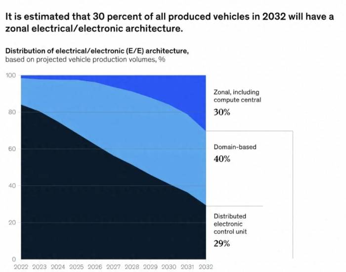
The next-generation electrical/electronic (E/E) architecture of Software Defined Vehicles (SDV) is evolving towards centralization. McKinsey analysis estimates that by 2032, 30% of all cars produced globally will adopt an E/E architecture with regional controllers. For the semiconductor industry, it is crucial that this shift will require centralized high-performance computing units.
Within the next decade, the automotive microcomponent and logic semiconductor market is expected to grow to $60 billion by 2032. The entire automotive semiconductor market is anticipated to grow from $60 billion to $140 billion over the same period. Its compound annual growth rate of 10% exceeds all other vertical markets in the semiconductor industry.
Centralized high-performance computing units typically provide functions for advanced driver-assistance systems (ADAS) or future autonomous driving (AD), as well as infotainment and vehicle motion tasks. Two prototypes—stand-alone, domain-specific computing units, and cross-domain central computing units—will dominate the next-generation E/E architecture. Depending on this nature, OEMs and Tier 1 suppliers can implement centralized computing units in various ways, such as through rack-based setups, printed circuit boards (PCBs) with multiple chips, or fusion chips for multiple domains.
Advertisement
In all cases, selecting the most efficient underlying system-on-chip (SoC) or system-in-package (SiP) is crucial for the following reasons:
Firstly, SoCs and SiPs implement the fundamental computing required for autonomous vehicles (e.g., by enabling perception functions that recognize other vehicles and traffic participants), in addition to providing cutting-edge infotainment services and supporting generative artificial intelligence (gen AI) use cases (e.g., for in-vehicle assistants).
Secondly, SoCs and SiPs are major drivers of cost and greatly affect the overall bill of materials (BOM). Lastly, their power consumption may play a role in ensuring the energy-efficient operation of vehicles, which is particularly important for the transition to battery electric vehicles (BEVs).
As a result, automotive OEMs are highly invested in continuously improving computational power and efficiency. Consequently, two emerging trends in the ADAS/AD and infotainment sectors have gained attention during the conceptual phase of the upcoming E/E architecture: fusion chips and chiplet-based chip designs.This article will discuss the integration of chips and chiplet-based chip designs as driving factors for centralized computing in future E/E architectures, and discuss why they have become an important factor for Chief Technology Officers when making strategic decisions about centralized computing.
Advancing Centralized Computing in ADAS/AD and Infotainment Domains through Integrated Chips
Integrated chips can be seen as a logical next step in enhancing SDV functionality and computing integration. That is, integrated chips merge the functions of infotainment and ADAS/AD onto a single silicon chip, forming a singular "integrated" chip.
At first glance, the technical requirements for this integration seem reasonable. Today, both the ADAS/AD and infotainment domains require the most advanced multi-core central processing units (CPUs), graphics processing units (GPUs), AI accelerators, and digital signal processors, and both domains aim to be implemented at very small node sizes (i.e., less than 10 nanometers) to improve computing power and energy efficiency. At the same time, several aspects of this integration reveal the differences between the two domains:
While the infotainment domain has some applications related to functional safety (e.g., supporting the cockpit cluster), the demand for automotive safety integrity level B (ASIL-B) and ASIL-D functional safety compliance is more evident in the ADAS/AD domain, as this domain must perform many real-time critical functions (e.g., actuator control tasks). A pure safety island approach may not be sufficient here, as the infotainment usually adopts this approach.
In the ADAS/AD domain, the need for a close collaborative design of hardware/software (HW/SW) is particularly evident in order to optimize the computing hardware (e.g., AI accelerators) for specific neural network architectures of perceptual elements (e.g., convolutional neural networks and transformers).
In the past two years, despite the many challenges of integrated chip design, fabless semiconductor manufacturers and new entrants have turned this theoretical idea into reality. In addition, several Tier 1 suppliers have demonstrated the design of computing units using integrated chips and promoted their advantages in the SDV environment.
By using integrated chips, OEMs can reduce the total number of physical computing units and further simplify the overall integration and integration of computing logic. For example, this approach is crucial for promoting over-the-air (OTA) updates throughout the vehicle's life cycle, which is a key driving factor for SDV. In addition, OEMs can simplify the toolchain and development framework in the infotainment and ADAS/AD domains, which is expected to have long-term cost advantages.
McKinsey, in collaboration with the Global Semiconductor Alliance (GSA), conducted a survey of stakeholders in the entire automotive semiconductor value chain. Respondents indicated that convenient development models (such as development environments and toolchains) and cost reasons (such as saving intellectual property and packaging costs) are their top factors in deciding to adopt integrated chips that combine ADAS/AD and infotainment functions (28% and 57%, respectively).
At the same time, the transition to integrated chips will also bring some challenges. First, integrated chips require higher technical complexity (e.g., verification work) to ensure non-interference, as infotainment and ADAS/AD must be separated, and any computing requirements of one domain cannot interfere with the other domain. In addition, there will be an increase in the organizational burden in terms of the coordination needs between the infotainment and ADAS domains.The second issue is to meet the redundancy requirements of L3 and above autonomous driving systems. L3 level systems require conditional autonomous driving, computational redundancy, actuators (braking and steering), and power supply. When the computing functions of infotainment and ADAS/AD are combined on a highly integrated chip, it may not be necessary to deploy a second chip, because the infotainment domain does not require additional computing power in the event of a failure of the main chip. In this case, deploying a second chip may incur overhead.
An additional challenge is that due to the relevant functional safety requirements, the consistency requirements of electromagnetic compatibility (EMC) are more complex; there is limited possibility for separate optimization, such as functional safety requirements and dedicated accelerators; and the loss of the ability to choose the best suppliers for the two domains and a higher lock-in effect.
In the survey, participants also pointed out that the three major challenges faced by the integration of SoC are ensuring no interference (33%), dealing with organizational reasons (25%), and addressing the redundancy requirements of ADAS/AD (19%). Scalability in computing power and physical and manufacturing difficulties (13% and 10% respectively) are considered less challenging.
Considering the redundancy requirements of higher-level autonomous driving, the integrated chip may be a particularly feasible solution for deployment scenarios targeting L0 to L2 applications (such as adaptive cruise control [ACC], lane departure warning [LDW], and automatic emergency braking [AEB]), rather than scenarios targeting L3 and above applications (such as hands-off and eyes-off scenarios), especially before 2030. In addition, the integrated SoC may take over the functions between the two domains, such as driver monitoring and occupant detection—becoming increasingly important in view of the upcoming new car assessment program (NCAP) regulations in Europe.
In the field of infotainment, the integrated chip is very suitable for controlling a wide range of functions, such as the cockpit cluster, central stack and passenger display, augmented reality display, surround view parking, rear-seat entertainment, and electronic rearview mirror.
According to recent public announcements, the integrated chip for series vehicles is expected to be first deployed between 2026 and 2027, with the main adopters being cost-effective mass original equipment manufacturers and disruptors with limited technical legacy and more open to technological innovation.
Adopting Chiplet for Customized Automotive Chip Design
Broadly speaking, "Chiplet" refers to an advanced packaging form - an innovative technology used to enhance the performance, functionality, and integration of semiconductor devices, beyond traditional packaging methods. The chip set architecture represents a paradigm shift in semiconductor design, enabling the modular integration of multiple dedicated chips into one package. The chip set allows OEMs to choose the best technical solution for each sub-component, highlighting that not all components need to be manufactured at the cutting-edge node size. Therefore, chip set-based designs can be used in both dedicated ADAS/AD and infotainment chips as well as integrated chips.
Due to the flexibility achieved, people can even consider using chips when the overall chip design is to support different computing loads (for example, by using dedicated CPU chips). Therefore, regional controllers may also constitute an interesting application area, as their computing requirements vary by prototype (for example, simple input/output aggregators and mature computing units).
Not all functions of modern chips (such as CPU, memory, AI accelerator, serializer, and deserializer) are integrated on a single silicon chip, but each component of the chip set is implemented using the most suitable and economically feasible technology node size for the application. This means that CPU and accelerator subsystems may adopt the smallest available node size, while other functions may be implemented on larger node sizes. To ensure that separately manufactured components can still work together, a common interface standard is needed, such as the Universal Chiplet Interconnect Standard (UCIe). As described later, many efforts to create these standards are underway.In the automotive sector, experts most frequently mention two advantages of chiplet-based chip design:
Reduction in overall chip size. The use of chiplets avoids the increase in chip size (area) that comes with monolithic design methods. Over the past five years, the chip area of complex chips has been continuously increasing, almost reaching the extreme ultraviolet lithography mask limit of 858 square millimeters. For GPUs used in data centers, this issue becomes particularly prominent, as larger chip sizes allow for more transistors, thereby enhancing computational and processing capabilities. Remember that the yield of the process is limited by defect density (the number of defects per unit area), and larger chips are more likely to contain one or more defects because they cover a larger area. Even a single defect can cause the chip to malfunction. In the long run, smaller chip sizes can improve yield, thereby reducing costs.
While this effect is an important advantage of chiplets, automotive chips are not expected to reach such sizes before the mid-2030s. Instead, the Lego principle is more important for the automotive vertical industry.
The Lego principle (or modular chip design implemented by standards) allows automotive OEMs to mix and match components from an existing design pool or library to meet their specific needs. The benefits of this principle include the ability to reuse components. Since the manufacturing volume of the automotive industry is lower than other segments (for example, the annual production of cars is close to 100 million, while the shipment of smartphones is close to 1.5 billion), customizing and reusing components will improve the cost efficiency of the target chip design. Other benefits include accelerating the time to market for new chips, improving scalability by selecting components that are truly needed, and providing more supplier options for specialized chips such as accelerators.
Surveys show that the majority of respondents in the automotive semiconductor value chain (61%) state that the flexibility to design the best chips by mixing and matching or using the Lego principle is the main motivation for the industry to adopt chiplets. Reducing total operating costs and increasing the yield of individual IP components are seen as important advantages of chiplet-based designs, but have a smaller impact (19%).
The ecosystem is crucial for the success of chiplets. These ecosystems promote standardization and create an environment that encourages the adoption of chiplets in different vertical industries (such as data centers and automotive).
The UCIe standard is one of the most important advancements in the field of standardization. Since the release of the first standard (UCIe 1.0) in March 2022, we have established an automotive working group to contribute to the revision of the standard for automotive applications.
In addition to standardization, emerging ecosystems also play a role in promoting their adoption. For example, the Automotive Chiplet Consortium, sponsored by the independent nanoelectronics R&D center Imec, brings together more than 50 participants in the automotive semiconductor value chain to discuss and exchange ideas on the progress of automotive chiplet design.
Chiplet technology is still an emerging technology. OEMs must consider the challenges of using chiplets, especially when considering series deployment.Automotive Readiness: To meet automotive readiness, chip design must comply with all necessary equipment and manufacturing specifications (such as AEC-Q100 and IATF 16949), and be able to withstand harsh environments, including vibrations and temperatures. Compared to automotive manufacturing, current use cases in data centers offer a more stable environment and fewer challenges.
Interconnect Standardization: As mentioned earlier, ecosystem participants should consider establishing a common standard so that designs can be combined. Currently, major players in the industry are forming different alliances and standards. A global, widely accepted standard is crucial for realizing the concept of the Lego principle.
Adoption of New Development Paradigms and Openness: To ensure the successful adoption of chiplets, participants in the value chain (intellectual property, foundries, integrated device manufacturers, and packaging) can seek new cooperation models. Although all participants recognize this as a key element, it may be difficult to achieve in a timely manner. This is partly due to challenges in intellectual property and unresolved issues regarding responsibility, such as determining which party will be responsible for the overall reliable operation of the chip, while each party provides its building blocks. From the perspective of verification and validation, value chain participants believe that the mixed "store" chiplet creation method is impractical.
Most senior leaders in the value chain predict that chiplets will be more widely adopted in the next decade. In the survey, 48% of industry leaders expect chiplets for automotive applications to emerge between 2027 and 2030, while 38% predict it will happen between 2030 and 2035. Only 8% expect the technology to develop more quickly, between 2025 and 2027. Considering the overall growth and development time of the automotive industry, this delay is not surprising.
Furthermore, the transition to chips is expected to be gradual. Although the Lego principle is attractive, the first chip designs are likely to be homogeneous. In these designs, intellectual property modules will come from the same supplier and use proprietary or established standards, such as Peripheral Component Interconnect Express (PCIe). The next step is likely to be the design using building blocks from an external party, which also helps to address responsibility issues. True heterogeneous designs, with a real combination of multi-supplier or multi-technology node sizes, are likely to appear in the mid-2030s and beyond.
The importance of chip-based designs is evident, as they allow chips to bypass existing limits when computing demands increase while maintaining cost-effectiveness. Once the chip ecosystem and standards are in place, stakeholders should quantify the benefits and opportunities of current application scenarios.
The impact of integrated chips and chiplets on participants in the entire automotive semiconductor value chain
The rise of SDV and supply chain issues have prompted automotive OEMs to delve deeper into the semiconductor value chain. OEMs recognize that a comprehensive understanding of semiconductor technology to achieve the most advanced functions in the fields of autonomous driving and infotainment is crucial to maintaining competitiveness.
This trend affects all participants in the automotive semiconductor field, especially OEMs, tier-one suppliers, IDMs, and fabless participants. As mentioned earlier, the decision to adopt integrated chips is likely to be made within the next two to four years, while the issue of implementing chiplets may be further addressed in the future.
The automotive computing unit market is expected to grow from $96 billion in 2023 to $148 billion in 2030, with a compound annual growth rate of 6%.Specifically, the trend towards centralization and integration leads to limited growth in the body and chassis domain, with an annual increase of only 1% to 2%, and the powertrain unit may even slightly decline. Given that the functions of these units will be implemented in regional controllers or centralized computing units (such as the vehicle motion computing unit), these units may even experience a decline. The compound annual growth rates for ADAS/AD and infotainment units are 22% and 6%, respectively. The former is driven by an increasing number of vehicles with L2+ and above functions (such as hands-free, eyes-free, and conditional autonomous driving).
According to McKinsey analysis, the market value of regional controllers is expected to reach $3 billion by 2030, while the market value of centralized computing units (such as integrated SoCs and vehicle motion computing units) will reach $8 billion.
I. Impact on Original Equipment Manufacturers (OEMs)
When deciding whether to adopt an integrated SoC, OEMs should consider the following strategically significant areas:
Software expertise. Is there sufficient expertise and control over the software architecture of these two domains to meet integration requirements?
ADAS/AD. What level of autonomous driving should be supported, and what functions should be carried on the integrated SoC?
Governance. How are the infotainment and ADAS/AD groups set up? What is the feasibility of coordinating development and release schedules?
Procurement strategy. Will purchasing ADAS/AD and infotainment chips from the same supplier hinder any strategic procurement decisions and supply chain resilience themes?
BOM and total cost of ownership economics. How much cost can be saved on the basis of the Bill of Materials (BOM)? Considering the total cost of ownership and taking into account the requirements of the first few years of investment (such as new development models and new tools), what is the business case?On Chiplets, there are three feasible approaches: First, OEMs can simply rely on their IDM and fabless partners to drive the development of chiplets; second, OEMs can actively participate by joining standardization organizations (such as UCIe) and ensuring the inclusion of specific requirements; third, OEMs can actively develop chiplets on their own; however, this option requires a significant amount of resources, including the establishment of a dedicated professional team.
II. Impact on Tier-1 Suppliers
Tier-1 suppliers may follow the trend of integrated SoCs, using integrated SoCs to create their own centralized computing unit designs. They can use these designs to demonstrate potential technical and business benefits to OEMs. Several Tier-1 suppliers are implementing this strategy, preparing for production that will begin between 2026 and 2028.
The range of chip options provided by Tier-1 suppliers is similar to that of OEMs. Tier-1 suppliers may wish to engage with OEMs early on, incorporating their chip requirements into the development roadmap for the next generation of centralized computing units.
III. Impact on Foundries, IDMs, and Fabless Manufacturers
While the impact and rise of integrated chips are likely to have a limited effect on foundries, IDMs, and fabless manufacturers, the relevance of chiplets will raise broader issues regarding the responsibility and "ownership" of the chips ultimately manufactured. In addition to technical topics, the following strategic areas may be most relevant:
Ecosystem. Which ecosystems and standards are successful? Which standards are worth early investment and participation?
Intellectual Property Ownership. Who will hold the intellectual property "Lego blocks" used to manufacture the final chips?
Liability. Who will be responsible for the final functionality of the chips if issues only arise in the field? Moreover, is this party responsible for manufacturing the chips and handling interconnections, or is it the party providing the intellectual property?
Development. What additional tools and methods are needed to facilitate a multi-supplier chip ecosystem? How should the design verification and validation processes for chip-based systems change?Business Model. What are the pricing and licensing schemes like? Who will receive what compensation?
In the future, semiconductors will play an increasingly important role in centralized computing units. As a result, OEMs are delving deeper into the automotive semiconductor value chain and participating more actively in the selection of components, functions, and specifications. A thorough understanding of integrated chip and chip-based design technologies, their advantages and challenges, and potential considerations will enable stakeholders throughout the automotive semiconductor value chain to maintain flexibility and competitiveness in the next generation of software-driven vehicles.
Comments