At the recent launch event for the third-generation DPU hosted by Zhongke Yushu, Professor Zheng Weiming from Tsinghua University and Academician of the Chinese Academy of Engineering, first pointed out that currently, the world is entering an economic development period dominated by the information industry. The increasingly diverse and complex application scenarios have put unprecedented demands on computing power, which has become the foundation of the digital economy. The chip is the core of computing power and the key to enhancing it.
Among them, GPUs and CPUs, due to their innate advantages, have become indispensable components of data centers. With the development of the internet, a large amount of data has flooded into data centers to be processed by cloud computing, thus giving birth to the emerging thing DPU, which accelerates the processing of data entering and exiting the data center.
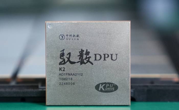
As a data processor, the DPU undertakes tasks such as data network transmission, storage, computing, and security, and is also known as the third main chip in the data center after the CPU and GPU.
Advertisement
Redefine DPU
"DPU is an important new type of computing power infrastructure, which will play an important role in future data centers, intelligent computing centers, and other high-bandwidth, low-latency, high-throughput products, providing core components for the construction of important new computing power infrastructure such as the east-west data calculation and computing power network," said Academician Zheng Weiming. Because of its importance, in the past few years, domestic and foreign companies have launched fierce competition in DPU, and Zhongke Yushu is one of the outstanding ones.
According to Mr. Cheng Ruiqi, Secretary of the Party Committee of Financial Street Capital, Chairman, and General Manager, Zhongke Yushu's team has actually started to invest in DPU research early on. As for the definition and function of this processor, it has also changed a lot in the past development in response to demand.
Yan Guihai, CEO of Zhongke Yushu, also frankly said that in the past, DPU was not new, and even it could be said that DPU was very old, old enough to be like a network card (also known as a network adapter), and its only function was to receive data from the Internet and send it to the local CPU.
"DPU is also very new, so new that we are called one of the important innovations in chip structure in the past ten years. On DPU, we see that it is no longer simply to realize the Internet function, but to reconnect the high-bandwidth, low-latency network between computing nodes. It can be said that with DPU, the computing power infrastructure has entered the high-speed train era from the green-skinned train era. Not only does it solve the connection problem, but it also solves the logical distance problem between nodes, virtual machines, and physical machines in the entire computing power infrastructure," Yan Guihai continued.
In the view of Zhongke Yushu, if the CPU is compared to the brain, then the GPU is like the muscle, and the DPU is the nerve center. The CPU carries the application ecosystem, which determines whether the computing system can be universal; the GPU provides high-density computing power of various accuracies, which determines whether the system has enough "strength"; the DPU is responsible for the efficient flow of data between various CPUs and GPUs, which determines whether the system can work collaboratively. After many years of development, the DPU has been close to the mature stage, which can provide us with the basic computing power of the network, data, storage, and security.
"In essence, the DPU is to solve the low efficiency of the CPU and the load that the GPU cannot handle. The multi-processing capability of the DPU will make it the core of the system," said Yan Guihai. From this, it can be seen that in response to the needs of the computing power center, Zhongke Yushu hopes to provide first-class DPU products to solve the problem of elastic expansion of computing power resources, solve the problem of efficient interconnection of all computing resources, and solve the problem of various computing offloading acceleration computing. Of course, the problem of unified operation and maintenance and unified control has also become the goal of Zhongke Yushu to solve.To achieve the aforementioned goals, it is necessary to start from three levels:
First, continue to strengthen architectural design, win with architecture, and redefine the DPU chip architecture with the most advanced chip architecture;
Second, enhance the software, import customer applications with the highest compatibility software;
Third, go to the platform, install the architecture and software on the demonstration platform, so that customers can access the DPU large-scale deployment at the lowest cost and carry out business verification;
"To achieve these goals, we see that the DPU is no longer just a chip, but an integrated system of chip, software, and platform, and it is an integrated project." said Yan Guihai. Based on this insight, Zhongke Yushu has built the company's DPU technical foundation.
Determine the technical route
Before introducing the technical foundation, let's take a look at some of Zhongke Yushu's thinking on the definition of DPU.
It is reported that when defining the DPU, the first problem Zhongke Yushu encountered was the choice of technical route. After comprehensively considering the company's technical accumulation, the current situation of the industry, and the development trend, Zhongke Yushu unanimously believed that the DPU is not a chip that can be realized by simply piling up cores and splicing processes. Therefore, "splicing architecture" has become the company's choice.
"Architectural innovation is not an option, but a must," Lu Wenyan emphasized. "Our thinking is to take theory first, use innovative system theory to guide complex chip design." Lu Wenyan continued. He further analyzed that Zhongke Yushu made two major underlying innovations:
The first is the underlying innovation, which is the independent research and development of the KPU architecture."Leveraging the entire team's over 15 years of architectural accumulation in the field of system architecture, we have innovatively proposed a unified computing architecture for specialized computing, the Kernel Processing Unit (KPU), based on the technology route of software-defined hardware. The KPU takes heterogeneous computing cores as the basic computational units. These computing cores are designed based on the most computationally intensive business of the upper-level applications, abstracted into core functions, and customized to achieve ultra-high performance," Lu Wenyan introduced.
The so-called software-defined, according to Lu Wenyan, refers to establishing a mapping relationship between the upper-level application computing and the lower-level processing cores through a weak compilation method. During further operation, different core functions are activated through a data flow-driven approach to complete the computation. It is reported that this architecture has three major advantages:
First, software is definable. Different core groups can be customized according to the characteristics of the application, which can integrate various business processes. DPU can integrate protocols such as network protocols, storage protocols, and security algorithms;
Second, it has ultra-high parallelism, which can fully support parallelism of business sets and data sets;
Third, it has ultra-strong performance because the data flow structure is a computation-intensive rather than a control-intensive structure, and it is also a clean memory architecture.
The second underlying innovation is the establishment of the first DPU instruction set architecture, KISA, on the basis of KPU.
"KISA has made a significant step in advancing the software-defined technology route towards a more feasible and executable direction. It has systematically solved the problem of mixed programming paradigms in domain-specific computing, making development more simple and efficient, and allowing every line of code to directly reach DPU computing power," Lu Wenyan introduced.
It is reported that KISA (Kernel-based Instruction Set Architecture) is a strong extension instruction set launched by Zhongke Yushu for the strong IO, strong data, weak control, and agile heterogeneous needs of DPU. It is the industry's first specialized instruction set for the DPU field. Unlike traditional CPU instruction sets, KISA is oriented towards data rather than control, high computational density rather than low computational density, and takes data flow as the basic operation unit, rather than bytes. More importantly, KISA supports agile heterogeneity at the instruction set level for the first time, implementing management and scheduling of various heterogeneous processing cores with a set of unified instructions.
Zhongke Yushu stated that currently, the KISA instruction set covers the KISA basic architecture, as well as DPU-specific processing extension instructions, including packet parsing, forwarding instructions, and table query instructions, etc. Based on KISA, it has already covered 25 major application scenarios, with hundreds of use cases, and has been fully verified.
It is also under the impetus of these two underlying innovations that Zhongke Yushu has launched the company's third-generation DPU, K2 Pro.An "All-Round Champion" Chip
When summarizing the features of the K2 Pro, Lu Yanwen stated outright that the company set "practicality wins, mass production is king" as the goal for this chip at the beginning of the project. Therefore, when designing the K2 Pro, Zhongke Yushu not only pursued how extreme a single function could be or how prominent a single performance indicator could be, but also regarded it as a balanced system project.
To achieve the above goal, the company has made extreme optimizations in six aspects for this chip:
Firstly, K2 Pro must be an advanced and easy-to-use network chip; therefore, Zhongke Yushu has not only brought very comprehensive basic network offloading for it but also added very perfect operational capabilities. In addition, this chip has been enhanced in network latency and high-order packet processing capabilities, achieving an end-to-end network latency at the industry-leading level of below 1.2us, successfully filling the domestic gap in low-latency network cards.
"The combination of programmable packet processing engine and basic network breaks through the traditional network's limitation of only doing layer two packet processing, providing users with more flexible packet parsing and analysis capabilities," said Lu Yanwen.
Secondly, K2 Pro must be a high-throughput data processing chip;
Lu Yanwen stated that the DPU business has distinct characteristics such as a variety of business types, high concurrency, and high sensitivity to latency. For this reason, Zhongke Yushu has created a DPU with high-throughput processing capabilities. "We have done a lot of research on the flow scheduling and isolation of this DPU, and have made many optimizations on flow identification and concurrency, making its performance degradation not significant under extremely high concurrency," Lu Yanwen continued.
Thirdly, K2 Pro must be a strong business offloading chip;
In the view of Zhongke Yushu, the DPU must be light control, rather than making a control chip comparable to the CPU. Based on this insight, the company has done a lot of fine scheduling of flows, with a series of technologies to lift the offloading amount of very complex business in the cloud from less than 20% to more than 90% in the DPU, greatly reducing the control tasks. In the service governance scenario, Zhongke Yushu's chip can also reduce the original governance latency of more than 400us to within 30us. This result, which has achieved a leap in quantity, leads the industry and has made a new breakthrough.
Fourthly, the DPU must be a flexible and scalable processing chip.According to Lu Wenyan, a major trend of DPU is that an increasing number of business processes will be handled on DPU. At the same time, with the upgrade of protocols, the tasks also increase. Therefore, CASNUM Technology consistently believes that DPU must be scalable. This is first reflected in its own programmability. To this end, in addition to the programmable engine, CASNUM Technology has also introduced several offloading engines such as the protocol analysis engine PPP and the universal algorithm engine CAE for the company's chips to better support protocol and algorithm upgrade processing.
Secondly, CASNUM Technology has also developed a high-speed DPU chip interconnection scheme to achieve chip-level interconnection and complete the expansion of computing power.
"Unlike traditional SoC interconnection, DPU has stronger requirements for the entire interconnection scale, latency, and especially business isolation. Therefore, we have independently developed the NoC architecture. This architecture can support hundreds of cores fully interconnected, can achieve point-to-point communication of less than 20 nanoseconds, achieve point-to-point bandwidth of 200G speed limit, and can achieve complete isolation, which is a very important feature in DPU isolation." Lu Wenyan said.
In addition, the chips of CASNUM Technology also provide a variety of schemes for integrating with external computing power chips, giving DPU more possibilities. For example, in the financial scenario, CASNUM Technology has tried to use DPU to fully offload the communication protocol and business algorithm execution in finance, achieving more than 10 times the performance of the existing scheme, which has subverted many people's views on DPU.
Fifth, the K2 Pro should also be a stable "management" chip, playing the role of the main device in the application, managing the upper-level virtual machines, starting and recycling, managing the virtual machine system loading, and managing various upper-level resources. Through multi-level consideration of stability, CASNUM Technology has made very detailed exception monitoring and recovery mechanisms on this DPU, allowing it to achieve nanosecond-level recovery in packet-level exceptions.
Sixth, DPU must have better performance in energy efficiency ratio. Because only better energy efficiency can make it widely used. To this end, CASNUM Technology has used all low-power conventional means, made many detailed optimizations from the business level, made more accurate power supply use shutdown, and achieved reduced area and frequency without affecting performance.
It is based on these multi-faceted considerations that CASNUM Technology has finally launched the first-class, advanced and easy-to-use full-function DPU chip K2 Pro DPU, and created leading products based on this.
Three series, six products
According to the introduction, this chip is also equipped on the six DPU card products of CASNUM Technology's "Swift" SWIFT, "Flexible" FLEXFLOW, and "Kung Fu" CONFLUX series, accurately supporting the sub-segment business scenarios. Among them, the "Swift" SWIFT series focuses on low-latency networks, including SWIFT-2200N and SWIFT-NDPP. First, looking at the SWIFT-2200N, thanks to the company's low-latency DMA, MAC, and full protocol stack offloading technology, SWIFT-2200N has achieved an end-to-end network transmission performance of less than 1.2μs, reaching the industry-leading level, which can provide an ultimate performance experience for financial computing, the Internet of Things and other scenarios; the SWIFT-NDPP product is a secondary development platform launched by CASNUM Technology for ultra-low latency demand scenarios, equipped with the first domestic independently developed commercial chip-level data offloading engine DOE, network offloading engine NOE, using programmable architecture and other technologies, supporting secondary development, and can be used as a technical base for financial ultra-high-speed trading, artificial intelligence, industrial Internet, video streaming and other fields.
The "Flexible" FLEXFLOW series is aimed at high-throughput lossless networks, including two products: FLEXFLOW-2200T and FLEXFLOW-2100R. The former is a high-bandwidth general network card product with a complete stateless network offloading engine, covering 10GE to 100GE network access requirements, providing a bottom-level support for the construction of the basic network of the data center; the latter is a product that supports RDMA hard offloading technology, supporting the construction of a complete 200G high-speed lossless data transmission network, which is a key link in accelerating the training and pushing business of large models in the AIGC era.The "Kung Fu" CONFLUX series for software-defined networking (SDN) is another leading product launched by Zhongke Yushu this time.
Like other series, the CONFLUX series also includes two products, namely CONFLUX-2200E and CONFLUX-2200. Among them, the CONFLUX-2200E product activates a powerful NP engine, supporting SDN network function offloading acceleration, and its 40Mpps and 200Gbps powerful forwarding capabilities can cover the vast majority of application scenarios in cloud computing; the CONFLUX-2200P product is a full-function DPU product built by Zhongke Yushu with all its strength, supporting the sinking and acceleration of network, storage, security, and computing services, and is a trump card for cloud-native network technology.
With the help of these products, Zhongke Yushu's strength has been recognized by customers. And by launching the core software development platform HADOS, the product landing has been accelerated. "If the key to 'performance' is the chip, then the core of 'usability and ease of use' is the software," said Zhang Yu, Senior Vice President of Zhongke Yushu.
He further pointed out that when building high-performance cloud data centers and smart computing centers, the "three U in one" computing power base is the technical core. For domestic customers, there are still three main pain points when deploying "three U in one" high-performance computing power centers on a large scale: high cluster upgrade migration costs, long cycles, and high learning thresholds; large-scale use, deployment, and operation and maintenance difficulties, and the construction of security and high availability is extremely challenging.
In response to the above pain points, the software platform that plays the role of a computing power operating system is the key to solving the problem. Therefore, in response to the core position of DPU demand, Zhongke Yushu launched the third major version of the company's DPU operating system HADOS (Heterogenous Agile Developing and Operating System).
It is reported that this version is the integration and precipitation of all software R&D investment of Zhongke Yushu in six years and extensive landing experience in various industries. It is also an important milestone for Zhongke Yushu and even the domestic DPU software R&D platform. Because with this system, we have a Chinese plan to compete with Nvidia and Intel in the DPU field.
As the only DPU application development platform with full ecological compatibility in the industry, the core code of HADOS 3.0 has exceeded 1.26 million lines, including 2,765 multi-level APIs such as network, computing, storage, and security, and provides a large number of out-of-the-box components and services. At the same time, the system is also compatible with mainstream 8 CPU platforms and 10 operating systems, including all domestic CPU platforms, such as Loongson, Phytium, Haiwei, Kunpeng, Shenwei, and Zhaoxin, as well as mainstream domestic operating systems.
Zhang Yu told Semiconductor Industry Observation that HADOS has become the most fully adapted, most competitive, and most deployed DPU software development platform in the industry in China, with a cumulative deployment exceeding the level of tens of thousands of cards. "The core barrier of a successful computing power chip company must be both soft and hard, with strong technical barriers in chip architecture and a complete ecologically compatible software moat that requires long-term investment. HADOS is the software moat of Yushu." Zhang Yu emphasized.
In conclusion, when talking about the company's future development strategy, Yan Guihai first pointed out that looking at the global development, foreign manufacturers' portrayal of DPU has actually stagnated, which is also the reason why Zhongke Yushu wants to redefine DPU. It is revealed that by 2025, Zhongke Yushu will continue to deepen the architectural design on the basis of completing K2-Pro, and then launch the K3 chip.K3 will be based on the KISA2.0 instructions and 14-nanometer technology, while integrating a RISC-V lightweight control core, with processing bandwidth reaching 800G. The latency will be below 1 microsecond, and power consumption will be reduced by 40% compared to the K2Pro. In terms of software, it will be upgraded from HADOS3.0 to HADOS4.0, and the HADOS open-source educational version will be made available to various partners. At that time, Zhongke Yushu will also launch the enterprise version 4.0 of the system, which will reach unprecedented heights in performance, functionality, and stability.
Looking back at the decades of development in the chip industry, Intel has honed itself into a representative enterprise in the CPU industry, while GPU has become an indelible label for NVIDIA. As the new wave of processors approaches, Zhongke Yushu hopes to become a representative enterprise in the DPU field, so that when people talk about DPU, they will think of Zhongke Yushu.
This is also the goal that every Zhongke Yushu person strives for.
Comments