As the effectiveness of copper continues to diminish, chip manufacturers are increasingly focusing on new interconnect technologies, laying the foundation for significant shifts in performance enhancement and heat reduction for future nodes and advanced packaging.
The introduction of copper interconnects in 1997 revolutionized the then-standard tungsten vias/aluminum wire metallization scheme. Dual damascene integration schemes replaced "dry" steps such as plasma etching and deposition with "wet" processes like electroplating and CMP. At that time, manufacturers were striving to minimize RC delay in the face of more complex interconnect structures.
Nearly three decades later, the semiconductor industry is at a similar crossroads. The continuously shrinking line dimensions are approaching the electron mean free path of copper. Barrier layers are consuming a larger share of the total available line width. The demand for copper alternatives is growing. However, like most fundamental changes, manufacturers hope to postpone this change as much as possible.
Advertisement
Results announced at the recent IEEE Interconnect Technology Conference show that there are still opportunities for optimizing copper.
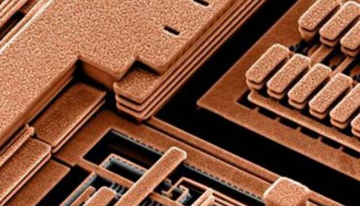
History of Copper Interconnects
Interconnects, the wires that transmit current between transistors, are a particularly concerning area. As chips become increasingly dense, interconnects need to handle greater tasks at smaller sizes. Before the advent of copper wires, aluminum was the ideal material for interconnects and the industry standard at the time, but its conductivity is quickly approaching its limits. In addition, aluminum wires are more prone to breakage.
Copper wires came to the fore at the right time.
In fact, everyone has known about the limitations of aluminum for a long time, and it is clear that the era of aluminum is obviously numbered. However, despite decades of research, no one has found a way to safely integrate copper into chip design. The main obstacle is to overcome the unsettling by-products produced by the interaction between copper and silicon. Unlike aluminum, copper effectively leaks atoms and destroys the electrical performance of silicon, which may lead to the unusability of silicon. "Copper is considered a killer of semiconductor devices," said Lubomyr Romankiw, an IBM Fellow and copper application expert, in the IBM Research Magazine. "The traditional view is to stay away from copper as much as possible."
To make copper interconnects feasible, three issues need to be addressed: determining how to chemically deposit it on the wafer in the best way, how to protect silicon from poisoning, and how to physically arrange copper on the chip.
IBM tested several methods of applying copper, including depositing solid copper from a gas suspension and using electricity to absorb copper ions from a liquid onto silicon, a process called electroless plating. Although the former method (called sputtering) initially looked promising, scientists ultimately chose the third option, electroplating, an impractical but familiar method - and surprisingly successful.To protect the silicon wafers, IBM scientists employed a stable metal studied by the company in the mid-1980s as a diffusion barrier against stray copper ions. The company designed a method to deposit the diffusion barrier along with copper onto the wafers. Researchers borrowed an etching technology invented by IBM in the early 1980s for its DRAM project.
This technology was named after the ancient metallurgists of Damascus, Syria, who perfected the metal inlay process. The so-called dual damascene method used for etching copper interconnects and vias was crucial to the success of the project. By removing the deposition and polishing steps from the typical manufacturing process, this method created a significant economic incentive for those seeking a viable copper solution.
Thus, by 1997, IBM unveiled a new type of semiconductor made of copper, which shocked the world. The successful application of copper in chip manufacturing, a goal that scientists had been unable to achieve for over 30 years, was realized. This breakthrough led to faster, cheaper chips and paved the way for the development of microprocessors. Due to the greater durability and reliability of copper wires, which are 100 times higher and can be scaled down to smaller sizes, the replacement of copper wires has led to an explosive growth of computing devices, from smartphones to automobiles.
Making full use of copper
However, after nearly thirty years, problems have emerged.
As interconnects shrink, the relationship between the interface and its properties and electrical performance is closer than the intrinsic material properties. Samsung Semiconductor Senior Engineer Jongmin Baek and his colleagues have specifically studied how to optimize the required barrier and etch stop layers for copper to improve overall performance. For example, in the contact metal-spacer test vehicle, the team used sidewall plasma pre-treatment to reduce the thickness of the sidewall barrier by one-third, thereby increasing the contact resistance by 2%.
Samsung researchers have paid particular attention to the via bottom barrier. Since the metal via is located on the metal wire, this barrier is not needed as an electrical insulator or diffusion barrier. It only exists as a product of the sidewall deposition, but it can account for more than 60% of the via resistance. Selective deposition methods are usually used to reduce the bottom deposition of vias. In Baek's work, the polymer inhibitor improved selectivity compared to the commonly used self-assembled monolayer, reducing resistance by 20%.
Modern interconnect schemes rely on various carbon-doped oxides to achieve the "C" part of the circuit RC delay. Materials with lower density have a lower dielectric constant (k), making them attractive. Other work by Samsung's Kang Sub Yim considered the consumption of carbon on the dielectric surface caused by plasma etching. The etching damage of low-k dielectrics increases the effective dielectric constant, thereby increasing the capacitance of the circuit. Materials with higher density (usually with k values above 3.0) are more resistant to plasma etching damage, which may make their effective k value lower in features below 30nm. For features smaller than about 30nm, the impact of surface carbon consumption is greater than the volume dielectric constant.The Yim team also utilized surface silicidation to repair etch damage. However, Baek pointed out that surface treatment on the dielectric sidewalls might contaminate the exposed metal at the bottom of the via. In contrast, the Baek team employed a proprietary chemical method's thermal recovery process, restoring the post-etch Si-OH terminated surface to a Si-CH3 terminated surface.
The full encapsulation of copper wires includes a metal capping layer (usually cobalt) to reduce electromigration, followed by an insulating etch stop layer and a blocking layer. Due to the reduction in spacing, the proportion of these layers in the total wire thickness is increasing. To improve the interface with the capping layer, Baek added plasma pre-treatment before the deposition of the etch stop layer. As a result, they found a 30% reduction in stress within the copper wires and a 10% reduction in via resistance. Additionally, Yim achieved similar results.
Ruthenium vias, followed by lines
While all these developments are promising, a long-term successor to copper is still needed. The via is dominating the overall interconnect resistance due to its small size and large quantity. In the first four to five interconnect layers, the metal wires are very short and do not generate much resistance. Therefore, an alternative is to use a transitional hybrid metallization scheme, combining copper wires with materials such as tungsten, ruthenium, or molybdenum for vias.
IMEC simulations indicate that using ruthenium vias in the first four layers of the interconnect stack can reduce the total resistance by up to 60%. To integrate ruthenium vias with copper wires, they suggest depositing a TaN blocking layer only on the dielectric sidewalls, placing ruthenium directly on the exposed copper. Any such scheme requires good dielectric surface passivation and good control of selectivity for ruthenium. Cluster tool processes are preferred because removing the native oxide from the exposed copper can damage the dielectric passivation.
Since ruthenium can be deposited or etched in various ways and does not require a blocking layer, it opens the door to more flexible integration schemes. For example, IMEC R&D engineer Giulio Marti and his colleagues benchmarked three different full self-aligned via processes.
The first and most traditional process uses EUV self-aligned double patterning, which creates spacer lines for defining metal wires (SADP-SIM). After transferring the spacer pattern to the SiN hard mask, selective RIE etching patterns the ruthenium metal layer, followed by SiO2 deposition. High selectivity etching aligns the via openings with the remaining SiN features, and then CVD ruthenium deposition is used to fill them.
The other two schemes considered by Marti are based on pillar vias, with a second layer of ruthenium deposited above the first layer, separated by an etch stop layer. In these schemes, pattern transfer uses a two-step ruthenium etch. First, a high aspect ratio etch cuts the required metal wires in both layers. Then, a spun-on dielectric fills these trenches, and a hard mask is placed on top. Tone-reversed EUV patterning of the hard mask protects the required via pillars, while the previous etch stop layer protects the underlying metal wires. Marti found that the two pillar via schemes increased the number of process steps but increased the process window. In particular, this method can prevent bridging between vias and adjacent lines.
Another IMEC R&D engineer, Chen Wu, and his colleagues proposed another alternative. They used SADP spacers (instead of metal) to define dielectric features. In this SADP-SID scheme, a hard mask material is deposited between the spacer pillars and then removed. Although this method increases process complexity, it means that the metal features are directly defined by the mask, providing designers with greater flexibility and control over feature sizes.Regardless of the specific methods, Wu emphasizes that optimizing the ruthenium etching and deposition process is crucial. The incomplete removal of the conical ruthenium profile, the base at the bottom of the ruthenium features, and the TiN adhesion layer will reduce the spacing between adjacent lines, leading to leakage.
Integrated schemes are just the beginning.
A successful process integration scheme requires careful attention to all component layers. For ruthenium, the optimization process has only just begun. Jack Rogers and his colleagues at the TEL Albany Technology Center have studied the impact of adhesion layer process conditions on the deposition behavior of ruthenium. Ruthenium films on PVD and ALD TiN have different grain orientations, different grain orientation distributions, and different resistivities. Larger and more uniform Ru grains seem to reduce resistivity, at least when the grains are smaller than the overall interconnect size.
Although the auxiliary layers required for ruthenium interconnects are fewer than those for copper (which is part of the focus), the reintroduction of metal etching and dielectric filling processes will undoubtedly keep process engineers busy for years to come.
Comments