PCIe, as a high-speed serial computer expansion bus standard, has long been popularized in every PC nowadays. Whether it is ordinary users or professionals, large companies or small businesses, everyone is enjoying the benefits brought by this standard.
However, this long-standing standard is not immutable. Over the past two decades, it has undergone six iterations, with the transmission rate per channel rising from 2.5 GT/s to 128 GT/s, achieving earth-shaking changes. The seventh generation is also steadily advancing, and everything seems to be thriving.
But in fact, over the years, Richard Solomon, the vice president of PCI-SIG (the organization responsible for controlling the development of the PCI-Express specification), has been hearing complaints - how long does this organization need to push the latest specifications to the industry. From the reactions of all parties at the recent PCI-SIG Developer Conference, it seems that everyone's patience is gradually being lost.
Advertisement
The foreign media Next Platform even bluntly stated that PCI-SIG needs to speed up its timetable and strive to keep the roadmap of PCI-Express synchronized with the roadmaps of chip manufacturers and server suppliers. For an industry that has a wide range of interconnects such as Ethernet, InfiniBand, and Nvidia's proprietary GPU built-in NVLink, it is expected that with the increase in the use of CXL-based hierarchical and shared main memory, the demand for PCI-Express will increase.
However, Next Platform also acknowledges that an organization with so many members (currently about 970 members and still growing) and a highly deliberate process for each specification may not be aimed at speed. There are countless committees and working groups in the specifications, which may lead to various changes, pre FYI and FYI tests, and compliance seminars.
Solomon also told reporters and analysts at the 2024 PCI-SIG Developer Conference held this week in Santa Clara, California, that all of this takes time.
However, a battle around PCIe 7.0 has already begun.
PCIe 7.0, coming soon
PCIe 7.0 is the next generation of computer interconnect technology, designed to increase the data transmission speed per pin to 128 GT/s, twice that of PCIe 6.0 at 64 GT/s, and four times that of PCIe 5.0 at 32 GT/s. This will allow a 16-channel (x16) connection to support a bandwidth of 256 GB/s in each direction at the same time (not including encoding overhead). Such a speed will be very convenient for future data centers and artificial intelligence and high-performance computing applications that require faster data transmission rates (including network data transmission rates).In order to achieve an impressive data transfer rate, compared with PCIe 5.0 and 6.0, PCIe 7.0 has doubled the physical layer bus frequency. In addition to this, the standard retains pulse amplitude modulation with four-level signaling (PAM4), 1b/1b FLIT mode encoding, and the forward error correction (FEC) technology that has been used in PCIe 6.0. In addition to these, PCI-SIG has stated that the PCIe 7.0 specification also focuses on enhanced channel parameters and coverage, as well as improved power efficiency.
Looking back at the development process of PCIe 7.0, its early work began in 2022. At the PCI-SIG Developers Conference that year, PCI-SIG announced the specification for PCI Express (PCIe) 7.0. By the 2023 conference, PCI-SIG had completed the first draft version 0.3 of the specification and subsequently distributed it to the members of the organization, marking the official start of the development of the PCIe 7.0 standard.
In April of this year, PCI-SIG released version 0.5 of the PCI-Express 7.0 specification to its members, which is the second draft of the specification and the final call for PCI-SIG members to submit new features to the standard. PCI-SIG used the latest update to reaffirm that the development of the new standard is still on track for the final version in 2025.
Examining this version of the specification, PCI-SIG has increased the maximum data rate to 128 gigatransfers per second (GT/s), improved energy efficiency, and maintained backward compatibility with previous generation specifications. It also retains the Flit Mode encoding and PAM4 signaling that started with PCI-Express 6.0.
"Our main focus is to maintain the PAM4 signal, to maintain the Flit mode we developed for PCI-Express 6.0, all of these, and really focus on doubling the speed," said Solomon. "Increasing the transfer rate to 128 gigatransfers per second is the key point. We first maintain backward compatibility. This is an important part of PCI-Express. Over the years, we have successfully launched all PCI-Express specifications. We have been working to improve energy efficiency, although I have to chuckle a bit, because you will see the transfer rate of 128 gigatransfers per second compared to our original transfer rate of 2.5 gigatransfers per second. Yes, it consumes more power than in 2003."
He said that the balance of features is also important, adding: "PCI-Express is not necessarily the fastest technology you can buy. It is definitely not the cheapest technology. But we try to achieve this balance of the best cost-performance ratio—striving to provide really high bandwidth, really reasonable implementation. So, the silicon technology you choose for the PHY is the PCB technology you choose."
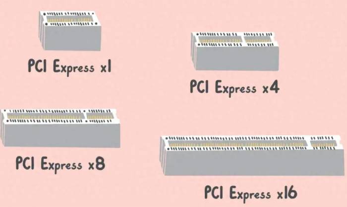
PCI-Express 7.0 also follows previous specifications, providing a range of options for it according to the product needs of the organization, as shown in the table below:
These options are the key points of PCI-Express.Solomon stated that the number of channels at the top of the chart is related to the area of the silicon wafer, and pointed out that 16 channels will occupy more silicon wafer space than two channels. However, you can achieve 16 channels with a cheaper process technology; two channels occupy less area, but achieving 128 GT/s may require a more expensive silicon wafer. "This just provides the ecosystem with a choice," he said. "You can choose the bandwidth, then see what is important for your specific product, and then choose the rectangle you want."
The next major step for PCIe 7.0 is to finalize the 0.7 version of the specification, which is considered a complete draft, where all aspects must be fully defined, and the electrical specification must be verified by test chips. After the release of this specification iteration, no new features can be added. PCIe 6.0 went through 0.3, 0.5, 0.7, and 0.9, four major drafts before finalizing, so PCIe 7.0 is likely to be on the same track.
It is worth mentioning that last summer, PCI-SIG announced the exploration of the possibility of PCIe fiber optic connections. To this end, the PCI-SIG Optical Working Group was established in August 2023, aiming to design appropriate outline dimensions for connectors and transceivers, and optical connection technology for data transmission through optical waves may expand the application field of PCI Express, such as cloud computing, high-performance computing, and quantum computing. Compared with copper wire transmission, this is expected to achieve higher throughput, lower latency, and lower energy requirements.
At the latest PCI-SIG Developer Conference in June this year, the organization stated that the logical layer and electrical layer of the PCIe 6.0 specification will accept the new standardization of optical PCIe, and PCIe 6.0 has already considered the use of fiber optic connections, which will improve the current PCIe electrical system instead of replacing it. This change is very likely to continue in PCIe 7.0.
Although the development of controller IP and initial hardware is already underway, it will take a few more years before the first actual mass production application of PCIe 7.0 hardware can officially meet everyone after the PCIe 7.0 standard is finalized in 2025.
The new battle has been ignited.
Although the official version of PCIe 7.0 will not be launched until next year, some manufacturers have already prepared their own solutions and IPs, intending to take the lead in the upcoming new standard popularization wave and capture more market share. At the recently held PCI-SIG DevCon 2024, each manufacturer brought out their latest technology, and the new battle has been ignited.
Alphawave Semi
At the PCI-SIG DevCon 2024, Alphawave Semi, as a high-speed connection and computing silicon supplier, demonstrated IP subsystem solutions for the rapid implementation of the next-generation PCIe 7.0 specification, as well as advanced technology that sets a new standard for the PCIe 6.0 technology ecosystem.
Alphawave Semi mainly showcased the PAM4 SerDes technology supporting DSP, which has laid the foundation for accelerating the time to market for emerging PCIe 7.0 solutions. It demonstrated how fully integrated controllers and top-level PAM4 SerDes PHY IP bring interoperable PCIe 6.0 technology connections for AI and high-performance computing (HPC) data center applications.Alphawave Semi has stated that its Silicon-Ready PipeCORE PCIe IP, in achieving the PCIe 7.0 standard, can be paired with Tektronix DPO70000 high-performance oscilloscopes to navigate transmitter performance at a speed of 128 GT/s (PAM4). This solution is backed by highly relevant models and laboratory measurements, ensuring a rapid entry into the market with a complete 128 Gbps solution.
Furthermore, Alphawave Semi has also demonstrated a complete PCIe 6.0 subsystem solution with an electro-optical link that breaks through the limit of 64 Gbps per channel. This integration includes Alphawave Semi's advanced controller IP and top-tier PAM4 SerDes PHY, as well as Innolight's LPO OSFP optical components. It has been stated that this technology can set new benchmarks for performance, energy efficiency, and latency in modern data centers, thereby driving the development of the PCIe 6.0 ecosystem.
Synopsys Technology
At the PCI-SIG DevCon, Synopsys showcased the world's first optical-based PCIe 7.0 IP, demonstrating the functionality of this technology in real-world scenarios. This includes the Synopsys PCI Express 7.0 PHY IP electro-optical-electrical (EOE) TX to RX operating at 128 Gb/s using OpenLight photonic ICs, as well as the successful implementation of root complex to endpoint connections and FLIT transmission using Synopsys PCIe 7.0 controller IP.
Synopsys's PCIe 7.0 IP solution is part of a broader portfolio for high-performance computing (HPC) SoC designs, which includes solutions for 1.6T/800G Ethernet, CXL, and HBM. It is understood that the main highlights of Synopsys's PCIe 7.0 IP solution include:
Complete Solution: Synopsys provides the industry's only complete PCIe 7.0 IP solution, including the controller, IDE security module, PHY, and verification IP. This solution can achieve bidirectional data transfer at up to 512 GB/s in an x16 configuration.
Energy Efficiency and Low Latency: The pre-verified PCIe 7.0 controller and PHY IP offer low-latency data transfer and up to 50% improved energy efficiency compared to previous versions, while maintaining signal integrity.
Security: The Synopsys IDE security module for PCIe 7.0 has been pre-verified with the controller IP, providing data confidentiality, integrity, and replay protection against malicious attacks, ensuring a secure data transfer environment.
Experience and Reliability: With over two decades of PCIe IP experience and more than 3,000 successful design cases, Synopsys offers a low-risk path to silicon success, providing customers with robust and reliable IP solutions.
Synopsys has stated that this solution is crucial for chip manufacturers to address the bandwidth and latency challenges brought by large language models and compute-intensive AI workloads. The company's PCIe 7.0 IP solution supports secure data transfer, alleviates data bottlenecks in AI workloads, and enables seamless interoperability within the ecosystem.John Koeter, Senior Vice President of IP Marketing and Strategy at Synopsys, said: "As a leading provider of interface IP, Synopsys continuously provides designers with the latest interfaces at the most advanced nodes, helping them meet the demands of compute-intensive designs. Synopsys' PCI Express 7.0 IP will offer customers a complete, standards-based solution, enabling them to start next-generation HPC and AI designs early and accelerate the path to silicon success."
Rambus also officially announced the launch of its own PCIe 7.0 IP product portfolio at the PCI-SIG DevCon, which includes a comprehensive set of IP solutions: the PCIe 7.0 controller is designed to provide the high bandwidth, low latency, and robust performance required for next-generation AI and HPC applications; the PCIe 7.0 retimer, for highly optimized, low-latency signal regeneration data paths; the PCIe 7.0 multi-port switch with physical awareness to support various architectures; and XpressAGENT™ to help customers quickly launch their first chips.
It is understood that the main features of Rambus' PCIe 7.0 controller IP include: support for the PCIe 7.0 specification, including a 128 GT/s data rate; implementation of low-latency forward error correction (FEC) for link robustness; support for fixed-size FLITs for high bandwidth efficiency; backward compatibility with PCIe 6.0, 5.0, 4.0, etc.; the most advanced security through the IDE engine; and support for AMBA AXI interconnects.
Neeraj Paliwal, Senior Vice President and General Manager of Silicon IP at Rambus, said: "With the emergence of new data center architectures, the landscape of data center chip manufacturers is booming, and high-performance interface IP solutions are needed to foster a strong and thriving ecosystem. The Rambus PCIe 7.0 IP product portfolio addresses this challenge by providing unparalleled bandwidth, low latency, and security features. These components work together to provide a seamless, high-performance solution that meets the strict requirements of AI and HPC applications."
Cadence also showcased its complete PCIe 7.0 solution at the latest PCI-SIG DevCon, especially the receiver and transmitter functions of its 128GT/s SerDes IP, demonstrating excellent electrical performance and margin. Cadence stated that its PCIe 7.0 subsystem test chip board can successfully transmit and receive 128GT/s signals through non-retiming optical links configured in an external loopback mode, with a significant margin.
Cadence also made several demonstrations at the event, including the powerful performance of Cadence IP for PCIe 7.0 in transmitting and receiving 128GT/s signals on non-timing optics, measuring the capabilities of Cadence IP for PCIe 7.0 using oscilloscope instruments, detailing its stable electrical performance and margin, identifying the PHY receiver quality of PCIe 6.0 interface Cadence IP using test equipment, and the reliability of Cadence IP for PCIe 6.0, as well as the PCIe 6.0 Cadence IP subsystem compliant with the PCI-SIG standard, optimized for power consumption and performance.
Cadence stated that it is the first IP provider to offer complete subsystem solutions for PCIe 3.0, 4.0, 5.0, and 6.0 with industry-leading PPA, and the company is proud to continue this trend with the latest PCIe 7.0 IP subsystem solution, setting new benchmarks for power consumption, performance, area, and time to market.
A review from 1.0 to 6.0PCI technology first appeared in 1992, supporting a peak throughput of 133 MB/s and a clock speed of 33 MHz, and quickly became the standard bus for connecting computer system components. Subsequently, in 1998, PCI-X (PCI Extension) provided the higher bandwidth required by the industry.
In 2004, a group of Intel engineers established the Arapaho working group to begin formulating a new standard, and later, other companies joined this group as well. Before officially determining PCI Express (PCIe), the new standard considered multiple names. To some extent, PCIe is the successor to PCI because it has similar functions, but PCIe is actually a completely different design from PCI. It is more like a network on the board, rather than the many old parallel interfaces of the PCI era. Ultimately, the industry successfully moved towards the PCIe 1.0 standard that year.
The initial standard, PCIe 1.0a, has a data transfer rate of 250MB/s per channel, with a total transfer rate of 2.5GT/s (gigatransfers per second). Like other serial buses, performance is usually measured in the number of transfers per second to avoid counting overhead bits as "data." PCIe 1.0a uses an 8b/10b encoding scheme, so only 80% of the transmitted bits are actual "data." Overhead bits have two main functions. First, they ensure that the serial interface always has enough clock transitions to recover the clock. Second, they ensure that there is no net direct current.
Subsequently, the PCIe standard began regular upgrades, with its transfer rate continuously increasing. Since PCIe is mainly used in personal computers and servers based on Intel processors, in practice, once Intel releases a processor that uses PCIe, the new standard takes effect. The overall idea of the standard evolution is to choose a transfer rate that can be manufactured on the mainstream process node at the time. However, because PCIe is ubiquitous, most designs that require a high-performance peripheral bus will use PCIe, regardless of the underlying architecture, such as the PCIe requirements specified in the Arm server base system architecture specification.
PCIe 2.0, launched in 2007, doubled the transfer rate, but the encoding scheme remained unchanged. Its bandwidth doubled, and it was compatible with the PCIe 1.0 standard. In addition, it improved the processing of the data link layer, supported more efficient power management, and enhanced data integrity and signal transmission stability.
PCIe 3.0, introduced in 2010, adopted a more efficient 128b/130b encoding scheme and added a scrambler function for known binary polynomials, achieving a good balance between 0s and 1s in clock recovery and zero direct current bias. This also greatly increased the transfer rate, with a 16-channel PCIe 3.0 interface reaching a maximum transfer rate of 15.7 GB/s. Today, PCIe 3.0 is the most widely deployed version of PCIe in market-available devices. For example, Google's third-generation TPU uses PCIe 3.0, and the widely used USB4 standard is also based on PCIe 3.0.
PCIe 4.0 standard was first introduced in 2017, offering a throughput of 64 GBps, with bandwidth continuing to double, maintaining compatibility with PCIe 3.0, while strengthening channel management and error detection mechanisms, and adding support for higher bandwidth requirements, such as for high-performance storage and network applications. However, it was not used for SSDs until 2019. The AMD Ryzen 3000 series CPU, first introduced in July 2019, was the first desktop CPU to support PCIe 4.0 x16 out of the box. To achieve full support, users need a new motherboard running the X570 chipset.
The PCIe 5.0 standard was released in May 2019, bringing a throughput of 128 GBps, while improving signal integrity and bit error rate (BER) control, and supporting higher-performance devices, such as GPUs for artificial intelligence and high-performance computing (HPC). The specification is backward compatible with previous generations of PCIe, and Intel was the first company to adopt PCIe 5.0 on its CPU, with its Alder Lake platform supporting the PCIe 5.0 standard.
The PCI-SIG, which defines the PCIe standard, had anticipated that PCIe 4.0 and PCIe 5.0 would coexist for a period, with PCIe 5.0 used for high-performance requirements that require maximum throughput, such as GPUs for AI workloads and network applications. Therefore, PCIe 5.0 will mainly be used in data center, network, and high-performance computing (HPC) enterprise environments, while lower-intensity applications (such as those used on desktop computers) can use PCIe 4.0.The PCIe 6.0 standard released in 2022, which is currently the latest, has once again doubled its bandwidth, significantly increasing to 8 GB/s per lane, and has also achieved tremendous changes in interconnectivity:
PAM-4 Electrical Signal Modulation Scheme: Instead of using the traditional non-return-to-zero (NRZ) signal, it adopts a pulse amplitude signal with four voltage levels, capable of generating a three-eye diagram. Pre-encoding and forward error correction (FEC) can respectively reduce analog and digital errors. This scheme can provide a bandwidth of 64GT/s with low latency.
FLIT Data Packet Transmission: This new data packet transmission architecture (required by FEC) not only supports increased bandwidth but also enables the system to handle the increased bandwidth.
L0p Low Power State: When the bandwidth demand in the system decreases, the new L0p low power state allows some lanes to enter sleep mode, which can optimize power consumption while ensuring that the link is always on.
Data Integrity and Security Protection: The specification uses Data Object Exchange (DOE) as a PCIe security building block at a lower bandwidth level, and uses encrypted data and keys. Component Measurement Authentication (CMA) provides firmware encryption signatures. Integrity and Data Encryption (IDE) provides packet-level security protection for the system to prevent physical attacks. By coupling IDE with the controller, it can provide efficient security protection at high bandwidth speeds of 64GT/s.
Although we are sparing no effort in promoting new technologies, I would like to ask a question, how long will it take for us to see the official launch of PCIe 6.0 products?
Comments